Semiconductor device and method of manufacturing the same

Active Publication Date: 2010-02-18
SEMICON COMPONENTS IND LLC
View PDF6 Cites 32 Cited by
  • Summary
  • Abstract
  • Description
  • Claims
  • Application Information

AI Technical Summary

Benefits of technology

[0020]Furthermore, the semiconductor device is completed as a die at the time of separation into individual semiconductor devices in the invention, different from the conventional where a plurality of components is manufactured separately and a semiconductor device

Problems solved by technology

Therefore, there is a problem of difficulty in making the whole size smaller.
Furthermore, since it is necessary to perform an assembling work (e.g. a process of disposing the LED die 102 on the first lead 101, a process of connecting the LED die 102 to the second lead 104 using the bonding wire 103, a process of sealing the whole with the transparent resin 106 and so on) after each of the components is completed separately, there is a problem of complex manufacturing processes and an increased cost.
Furthermore, like the semiconductor device 100, it is necessary to perform an assembling work

Method used


Image

  • Semiconductor device and method of manufacturing the same
  • Semiconductor device and method of manufacturing the same
  • Semiconductor device and method of manufacturing the same

Examples


first embodiment

[0047]the invention will be described referring to figures. FIGS. 1 to 14 are cross-sectional views in manufacturing process order.

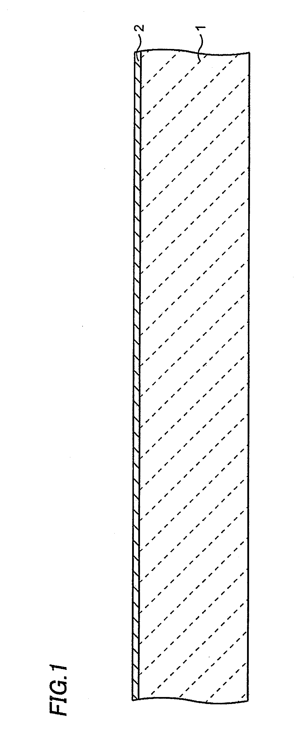
[0048]First, as shown in FIG. 1, a conductive layer 2 made of aluminum (Al), copper (Cu) or the like is formed on a front surface of a first substrate 1 to have a thickness of, for example, 1 μm by a deposition method such as a sputtering method or the like. The conductive layer 2 is a layer that is to be patterned into cathode electrodes 10 as described below. The first substrate 1 may be a semiconductor substrate made of silicon (Si) or the like, or may be an insulating substrate made of glass or the like.

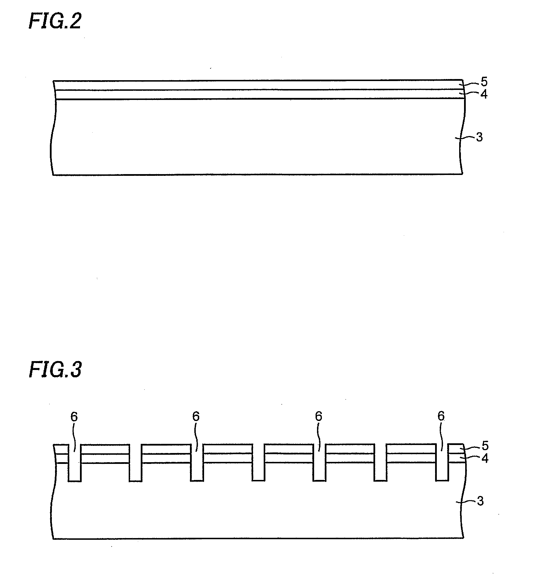
[0049]Then, as shown in FIG. 2, an N type second substrate 3 made of, for example, gallium arsenide (GaAs), gallium nitride (GaN) or the like is provided. The thickness of the second substrate 3 is about 300 to 700 μm, for example. The material of the second substrate 3 may be appropriately changed according to a target color of emission light. An N t...

second embodiment

[0076]Although the conductive layer 2 is patterned into the pad electrodes 33 and the cathode electrodes 10 after the LED dies 8 are transferred to the semiconductor substrate 31 in the second embodiment, the conductive layer 2 may be patterned before the LED dies 8 are transferred thereto instead. According to needs, a passivation film (not shown) (e.g. a silicon nitride film formed by a CVD method) covering the pad electrodes 33 partially or completely may be formed on the front surface of the semiconductor substrate 31.

[0077]Then, the insulation layers 11 covering the side surfaces of the LED dies 8 and parts of the cathode electrodes 10 are formed. The anode electrodes 12 are then formed so as to extend from on the front surface of the first substrate 1 onto the front surfaces of the P type semiconductor layers 5 along the circumferences of the insulation layers 11.

[0078]Then, as shown in FIG. 17, the semiconductor substrate 31 and the supporting body 16 are attached with the ad...

third embodiment

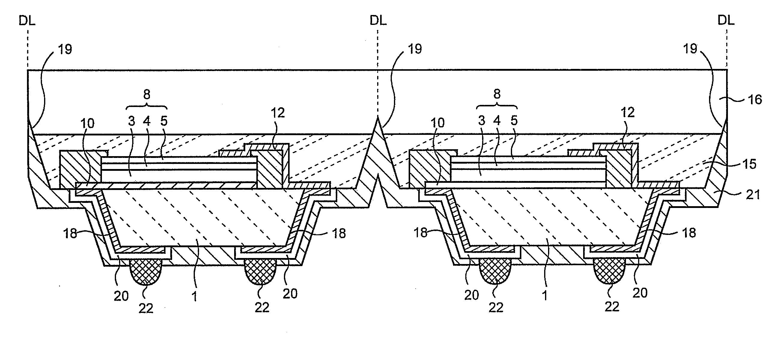
[0085]In the semiconductor device 50 of the third embodiment, as shown in FIG. 22, a light receiving element 51 is formed on the semiconductor substrate 31. The light receiving element 51 includes a photodiode (Photo Diode), a phototransistor (Photo Transistor) or the like that are generally known, and has a function of converting light into an electric signal. A metal layer 52 that reflects light emitted from the LED die 8 to the light receiving element 51 side is formed between the supporting body 16 and the adhesive layer 15. The metal layer 52 is preferably made of a material with high reflectance such as aluminum (Al) or the like, and may be formed on the attachment surface of the supporting body 16 by, for example, a sputtering method before the attachment of the supporting body 16.

[0086]The feature of the semiconductor device 50 of the third embodiment is that the light receiving element 51 is formed on the substrate (the semiconductor substrate 31) in addition to the light e...


PUM


Abstract

The invention is directed to providing a smaller semiconductor device with a lower manufacturing cost and higher reliability and a method of manufacturing the same. A light emitting element (a LED die 8) is formed on a first substrate 1. A cathode electrode 10 connected to an N type region of the LED die 8 is formed between the first substrate 1 and the LED die 8. The side surface of the LED die 8 is covered by an insulation layer 11. An anode electrode 12 is formed extending from on the front surface of the first substrate 1 onto a P type region of the LED die 8 along the circumference of the insulation layer 11. Wiring layers 18 electrically connected to the cathode electrode 10 and the anode electrode 12 are formed on the side surface of the first substrate 1 therealong. The wiring layers 18 extend onto the back surface of the first substrate 1. Conductive terminals 22 electrically connected to the wiring layers 18 through electrode connection layers 20 are formed on the back surface of the first substrate 1.

Description

REFERENCE TO RELATED APPLICATIONS[0001]This application is a national stage application under 35 USC 371 of International Application No. PCT / JP2008 / 051898, filed Jan. 30, 2008, which claims priority from Japanese Patent Application No. 2007-023878, filed Feb. 2, 2007, the contents of which are incorporated herein by reference.BACKGROUND OF THE INVENTION[0002]1. Field of the Invention[0003]The invention relates to a semiconductor device having a light emitting element and a method of manufacturing the same.[0004]2. Description of the Related Art[0005]A light emitting diode (LED: Light Emitting Diode) can generate light stably for a long time with relatively low electric power, and is generally used as a light emitting element. A conventional semiconductor device having a light emitting element will be described referring to FIGS. 25 and 26.[0006]As shown in FIG. 25, a conventional semiconductor device 100 has a first lead 101 (a cathode), a light emitting element (a LED die 102) hav...

Claims


Application Information

Patent Timeline
IPC IPC(8): H01L33/00H01L31/00H01L33/44H01L33/48H01L33/62
CPCH01L33/44H01L33/486H01L33/62H01L2933/0066H01L2224/48247H01L2224/48091H01L2924/00014
Inventor NOMA, TAKASHI
Owner SEMICON COMPONENTS IND LLC
Why Eureka
Try Eureka