Piezoelectric component and manufacturing method thereof

a technology of piezoelectric components and manufacturing methods, applied in piezoelectric/electrostrictive transducers, device material selection, generators/motors, etc., can solve the problems of extreme difficulty in miniaturization and warping of the overall piezoelectric substrate, and achieve the effect of reducing the size of the piezoelectric component, increasing the number of piezoelectric elements, and high functionalization

a technology of piezoelectric components and manufacturing methods, applied in piezoelectric/electrostrictive transducers, device material selection, generators/motors, etc., can solve the problems of extreme difficulty in miniaturization and warping of the overall piezoelectric substrate, and achieve the effect of reducing the size of the piezoelectric component, increasing the number of piezoelectric elements, and high functionalization

US20100045145A1Inactive Publication Date: 2010-02-25NIHON DEMPA KOGYO CO LTD

Image

  • Piezoelectric component and manufacturing method thereof
  • Piezoelectric component and manufacturing method thereof
  • Piezoelectric component and manufacturing method thereof

Examples


Embodiment Construction

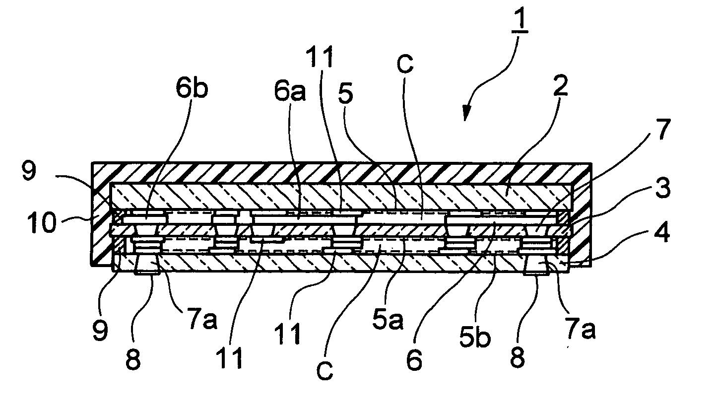
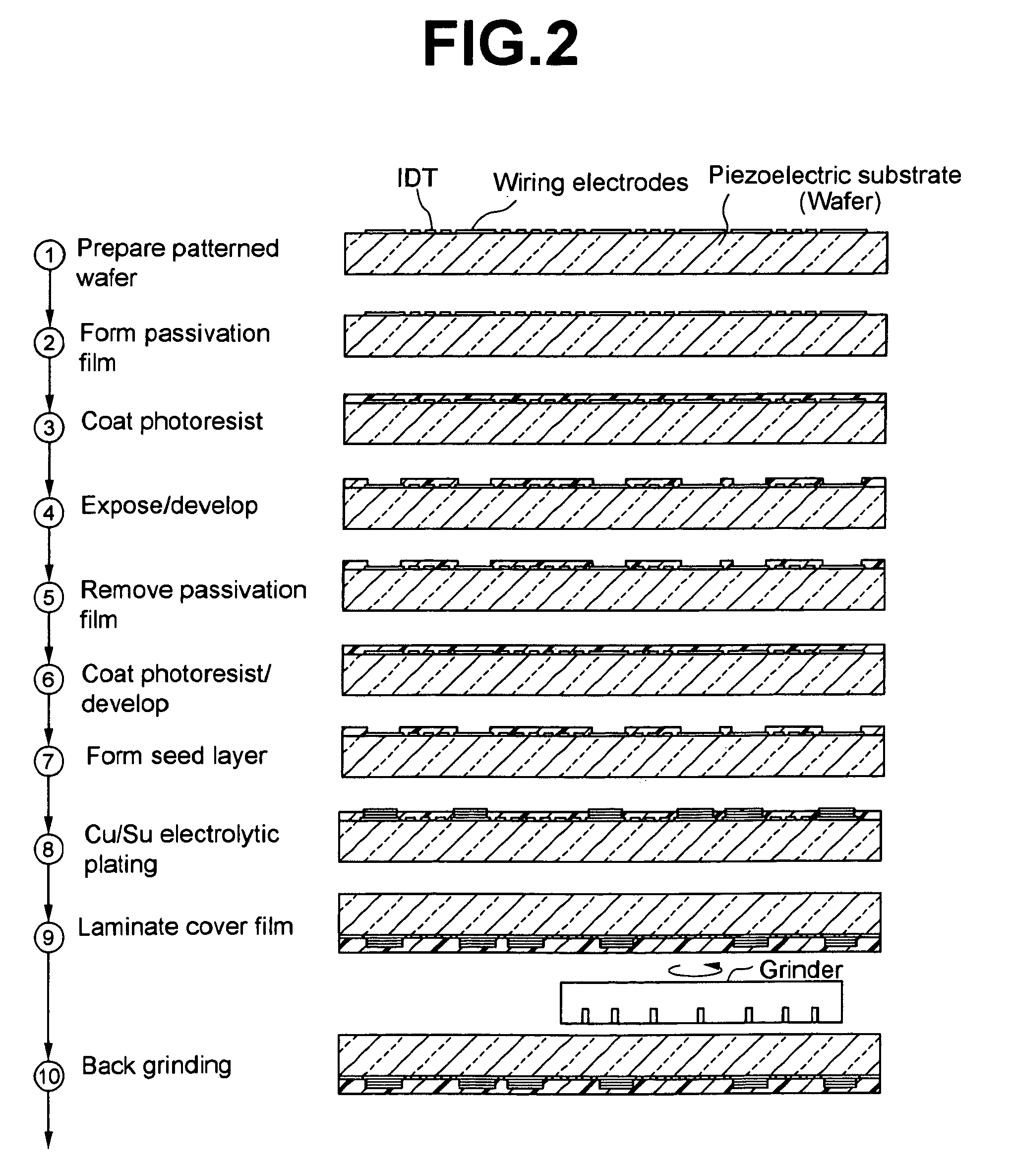
[0015]Hereunder, a piezoelectric component and a manufacturing method thereof of the present invention are described for an embodiment of a SAW device.

[0016]Piezoelectric Component (SAW Device)

[0017]FIG. 1 shows a SAW device, which is an embodiment of a piezoelectric component of the present invention.

[0018]This SAW device 1, as shown in FIG. 1, comprises: piezoelectric substrates (wafers) 2, 3, and 4 bonded and laminated so as to form hollow sections C between a plurality, for example, three of principal surfaces having a piezoelectric function formed on a piezoelectric substrate or a substrate of lithium tantalite (LiTaO3), lithium niobate (LiNbO3), quartz, or the like; comb-teeth (IDT) electrodes 5, 5a, and 5b made from an aluminum film that are formed on the principal surfaces of these piezoelectric substrates 2, 2, and 4 by means of deposition or sputtering; wiring electrodes 6, 6a, and 6b that have element wirings and that connect between the comb-teeth electrodes 5, 5a, and 5...


PUM

PropertyMeasurementUnit
thicknessaaaaaaaaaa
piezoelectricaaaaaaaaaa
thicknessaaaaaaaaaa

Abstract

An object of the present invention is to; miniaturize, increase the capacity, and reduce the price of piezoelectric components. The present invention relates to a piezoelectric component and a manufacturing method thereof, characterized in that: there are bonded and laminated at least two or more piezoelectric elements in which comb-teeth electrodes, wiring electrodes having element wirings that are arranged adjacent to the comb-teeth electrodes, and electrode terminals connected to the wiring electrodes, are formed on a principal surface of a plurality of piezoelectric substrates, while forming hollow sections between the respective piezoelectric elements; through electrodes are formed in the respective piezoelectric substrates so as to pass therethrough; the through electrodes are connected to the electrode terminals; and the piezoelectric substrates are sealed by a resin sealing layer.

Description

BACKGROUND OF THE INVENTION[0001]The present invention relates to a piezoelectric component such as a piezoelectric thin film and a surface acoustic wave (SAW) device used in a SAW duplexer and a SAW filter, to be used in mobile communication devices such as mobile phones, and a manufacturing method thereof. In particular, the invention relates to a piezoelectric component and a manufacturing method thereof in which at least two or more piezoelectric elements are flip-chip mounted on a plurality of wafers at a wafer (piezoelectric substrate) level, and these piezoelectric elements are laminated via a resin sealing layer and terminal electrodes while forming hollow sections between the piezoelectric elements, and packaged in a chip size.[0002]For example, in a piezoelectric component (SAW device) mounted in a mobile phone, around the comb-teeth electrode sections thereof [IDT (Inter-Digital Transducer) electrode sections], there are needed predetermined hollow sections.[0003]Conventi...

Claims


Application Information

Patent Timeline
25 Feb 2010
Publication
US20100045145A1
IPC
H01L41/047; H01L41/22; H01L41/16; H01L41/083; H01L41/09; H01L41/18; H01L41/23; H01L41/29; H01L41/313; H01L41/337; H01L41/338; H03H3/02; H03H3/08; H03H9/02; H03H9/145; H03H9/17; H03H9/24; H03H9/25; H03H9/70; H03H9/72
CPC
H03H3/08; H03H9/059; Y10T29/42; H03H2009/0019; H03H9/1085
Inventors
TSUDA, TOSHIMASA