3D integrated circuit device fabrication using interface wafer as permanent carrier

a technology of integrated circuit devices and wafers, applied in the direction of solid-state devices, semiconductor/solid-state device details, instruments, etc., can solve the problems of general purpose substrate thinning techniques that do not allow the production of final substrates, and only work for silicon-on-insulator (soi) wafers

Active Publication Date: 2010-02-25
GLOBALFOUNDRIES US INC
View PDF17 Cites 17 Cited by
  • Summary
  • Abstract
  • Description
  • Claims
  • Application Information

AI Technical Summary

Problems solved by technology

One problem experienced in the fabrication of 3D integrated circuit devices is that general purpose substrate thinning techniques do not allow the final substrate to be produced with a controlled thickness that is thin enough to allow high-density through-silicon vias with reasonable aspect ratios to be realized.
However, this technique only works for silicon-on-insulator (SOI) wafers.
Further, even with an SOI wafer, this technique does not work for SOI circuits having structures that extend below the buried oxide, such as an embedded DRAM (e-DRAM) trench.
However, this technique greatly increases the manufacturing cost.
Such protection is required because, while the SOI wafer acts as an etch stop, it does not provide selectivity between the different substrates.
However, this technique does not allow the wafers to be thinned aggressively and creates uniformity problems.
Further, for integrated circuits that

Method used


Image

  • 3D integrated circuit device fabrication using interface wafer as permanent carrier
  • 3D integrated circuit device fabrication using interface wafer as permanent carrier
  • 3D integrated circuit device fabrication using interface wafer as permanent carrier

Examples


Embodiment Construction

[0017]Preferred embodiments of the present invention will be described in detail hereinbelow with reference to the attached drawings.

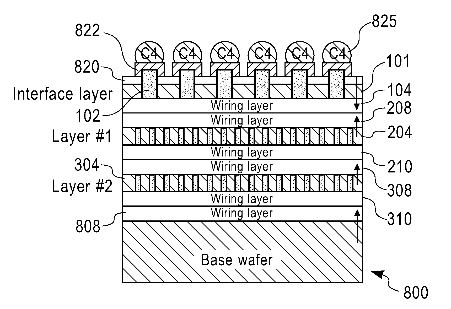
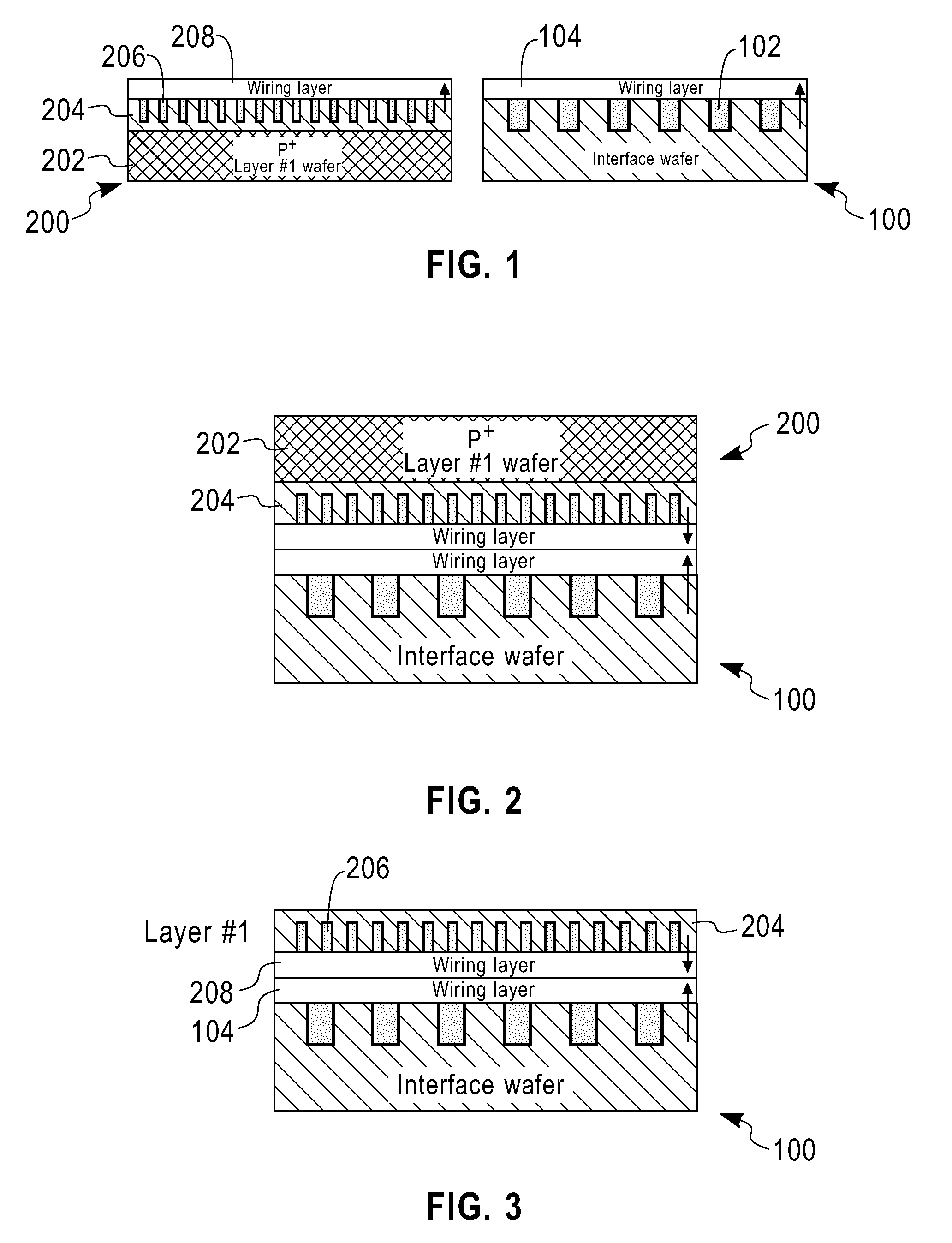
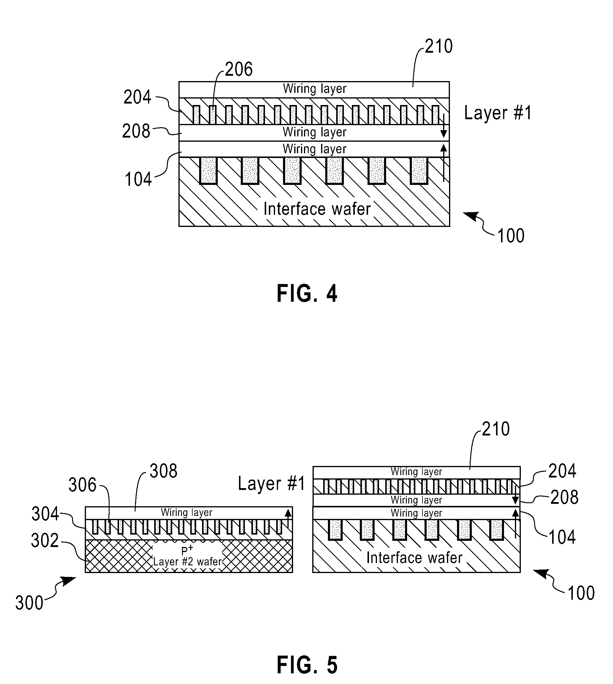
[0018]Embodiments of the present invention use the interface wafer as a permanent carrier during three-dimensional (3D) integrated circuit device fabrication. In one exemplary embodiment, the interface wafer is used during the stacking of the layers as a carrier for all of the layers of the stack except the base wafer. Thus, there is no need for layers to be bonded to temporary handle wafers. After the layers are stacked and attached to the base wafer, this carrier (i.e., interface wafer) is not discarded, but instead permanently remains as the interface between the stacked layers and the package in the 3D integrated circuit device. For example, in this exemplary embodiment the interface wafer has through-silicon vias at the same pitch as the package, and redistribution wiring that re-routes the leads to interface with the bottom layer in the stack. Th...


PUM


Abstract

A method is provided for fabricating a 3D integrated circuit structure. Provided are an interface wafer including a first wiring layer and through-silicon vias, and a first active circuitry layer wafer including active circuitry. The first active circuitry layer wafer is bonded to the interface wafer. Then, a first portion of the first active circuitry layer wafer is removed such that a second portion remains attached to the interface wafer. A stack structure including the interface wafer and the second portion of the first active circuitry layer wafer is bonded to a base wafer. Next, the interface wafer is thinned so as to form an interface layer, and metallizations coupled through the through-silicon vias in the interface layer to the first wiring layer are formed on the interface layer. Also provided is a tangible computer readable medium encoded with a program that comprises instructions for performing such a method.

Description

CROSS REFERENCE TO RELATED APPLICATIONS[0001]This application is related to application “3D Integrated Circuit Device Fabrication With Precisely Controllable Substrate Removal,” Ser. No. ______, now ______, and application “3D Integrated Circuit Device Having Lower-Cost Active Circuitry Layers Stacked Before Higher-Cost Active Circuitry Layer,” Ser. No. ______, now ______, which were filed on the same day as the present application and commonly assigned therewith to International Business Machines Corporation. These related applications are incorporated herein by reference in their entirety.[0002]This invention was made with Government support under Contract No.: N66001-04-C-8032 awarded by Defense Advanced Research Projects Agency (DARPA). The Government has certain rights in this invention.FIELD OF THE INVENTION[0003]The present invention generally relates to the field of integrated circuits, and more particularly relates to the fabrication of three-dimensional (3D) integrated cir...

Claims


Application Information

Patent Timeline
IPC IPC(8): H01L21/768G06F19/00
CPCH01L25/0657H01L2221/68377H01L2225/06513H01L25/50H01L2225/06593H01L2924/15311H01L2224/16H01L2225/06541H01L2924/37001H01L2224/92242H01L25/18H01L2224/0401H01L2224/05558H01L2224/0557H01L2224/131H01L2224/16227H01L2224/2919H01L2224/32145H01L2224/32225H01L2224/33181H01L2224/73153H01L2224/73253H01L2224/83121H01L2224/83895H01L2224/94H01L2924/10253H01L2924/14H01L2924/1431H01L2924/1433H01L2924/1434H01L2924/1436H01L2924/1437H01L2924/157H01L21/6835H01L2224/05024H01L2224/05008H01L2224/05009H01L2224/05568H01L2224/05001H01L2224/05144H01L2224/05147H01L2224/05155H01L2224/056H01L24/13H01L24/05H01L2224/73251H01L2224/08145H01L2224/83H01L2224/11H01L2924/014H01L2924/00014H01L2224/08H01L23/48H01L25/065
Inventor FAROOQ, MUKTA G.HANNON, ROBERTIYER, SUBRAMANIAN S.KOESTER, STEVEN J.LIU, FEIPURUSHOTHAMAN, SAMPATHYOUNG, ALBERT M.YU, ROY R.
Owner GLOBALFOUNDRIES US INC
Why Eureka
Try Eureka