Electronic component mounting structure and method for manufacturing the same
Inactive Publication Date: 2010-03-04
PANASONIC CORP
View PDF5 Cites 39 Cited by
Summary
Abstract
Description
Claims
Application Information
AI Technical Summary
This helps you quickly interpret patents by identifying the three key elements:
Problems solved by technology
Method used
Benefits of technology
Benefits of technology
[0013]Accordingly, it enables mounting with a low pressure at a portion where the photosensitive resin of the protrusion electrode is low in resin component crosslink density and absorbing stresses in application of the pressure, making it possible to improve the connection reliability and to efficiently prevent breakdown of the electronic component. Also, in connecting operation, fusion adhering of the conductive filler takes place at a portion of being low in resin component crosslink density of photosensitive resin, causing it to be metalized, and since the conductive fillers at a portion of being high in resin component crosslink density are in a state of contacting with each other, it is possible to decrease the connection resistance. Further, due to the portion of high resin component crosslink density, the strength of connection to the mounting substrate or semiconductor element increases and it is possible to realize an electronic component mounting structure which ensures excellent adhesion. Also, since fine protrusion electrodes can be formed by using photosensitive resin, it is possible to manufacture an electronic component mounting structure capable of meeting the requirement for narrower pitches.
[0015]Thus, it is possible to absorb stresses in the press-fitting step by making a portion being low in resin component crosslink density structurally porous, enabling the mounting with low pressing forces in the connecting operation, and it is possible to easily prevent breakdown of semiconductor element or generation of characteristic change. Also, conductive fillers at a portion of low resin component crosslink density of photosensitive resin are subjected to fusion-adhering (metalizing) and conductive fillers at a portion of high resin component crosslink density are subjected to contacting with each other, and therefore, the connection can be realized with low connection resistance. Also, since fine protrusion electrodes can be formed by using photosensitive resin, it is possible to manufacture an electronic component mounting structure capable meeting the requirement for narrower pitches at low costs.
[0017]In this way, protrusion electrodes varying in resin component crosslink density of photosensitive resin in the direction of height can be formed all together at predetermined intervals between the transparent connector terminal of the transparent mounting substrate and the electrode terminal of the electronic component. Accordingly, the steps of connecting the electronic component to the mounting substrate and forming the protrusion electrode can be performed at the same time, and it is possible to efficiently manufacture the electronic component mounting structure at low costs.
Problems solved by technology
However, in such a mounting technology with use of a solder bump, a high pressing force is required for press-fitting in the mounting step, causing a great load to be applied to the semiconductor element.
Therefore, in the case of recently available semiconductor element reduced in size having Low-K dielectric layer, there arises a problem such as breakdown of fragile dielectric layer, element breakage, or variation of semiconductor element characteristics.
However, in the semiconductor device of Patent document 1, there arises such a problem that the manufacturing cost becomes higher for forming a smaller-sized stress absorbing ball having a conductive member on the surface thereof.
Also, a bump electrode is formed by arranging a small-sized stress absorbing ball on the electrode terminal, and in this method, it is difficult to make the arrangement corresponding to the size reduced, making it difficult to realize high-density mounting.
Also, in the solder bump forming method of Patent document 2, since it is a mounting structure such that contact connection is made by pressing the solder bump having solder particles diffused in the resin and solder particles contacting with each other, there arises a problem such as generation of great electrical resistance and worsening of connection reliability.
Method used
Image
Click on the blue label to locate the original text in one second.
Reading with bidirectional positioning of images and text.
Examples
first preferred embodiment
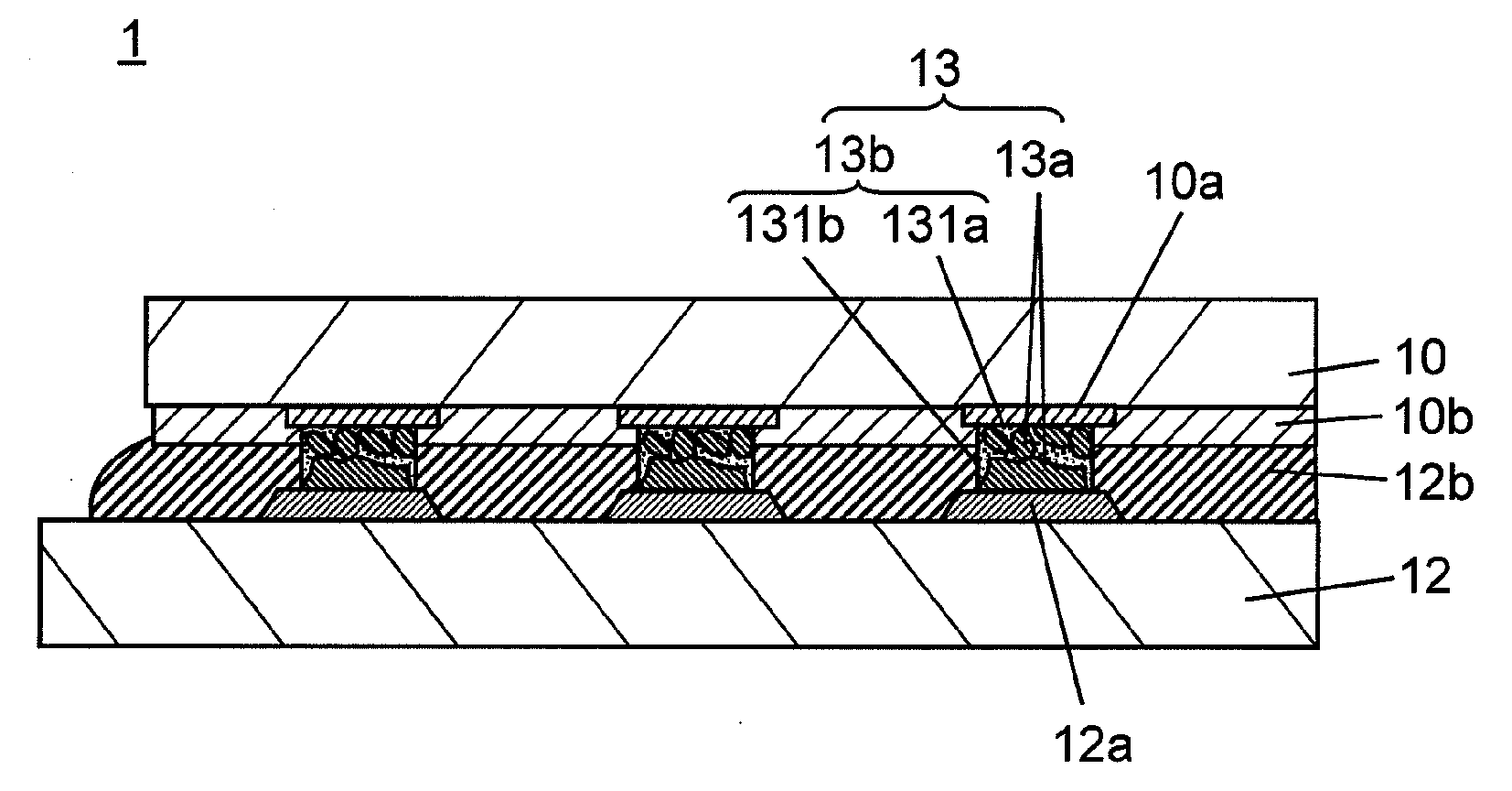
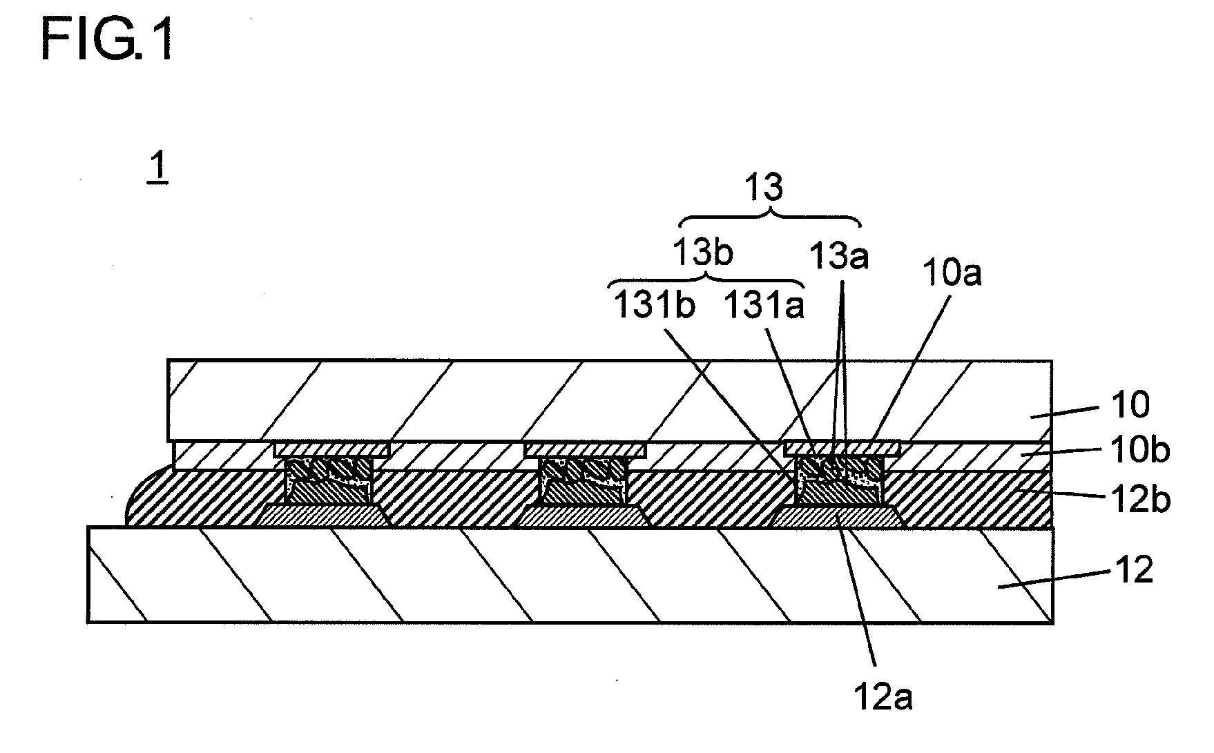
[0104]FIG. 1 is a conceptual cross-sectional view showing the configuration of an electronic component mounting structure in the first preferred embodiment of the present invention.
[0105]As shown in FIG. 1, electronic component mounting structure 1 comprises electronic component 10 having a plurality of electrode terminals 10a which is connected to mounting substrate 12 having connector terminals 12a facing to electrode terminals 10a by means of protrusion electrodes 13. In this case, electrode terminal 10a and connector terminal 12a are connected to each other in a fusion adhering or contacting fashion via protrusion electrode 13.
[0106]Also, protrusion electrode 13 includes at least conductive filler 13a and photosensitive resin 13b. Further, protrusion electrode 13 has such a structure that the resin component crosslink density of photosensitive resin 13b varies in the height direction of protrusion electrode 13. In this preferred embodiment, electrode terminal 10a of electronic c...
second preferred embodiment
[0149]FIG. 3 is a conceptual cross-sectional view showing the configuration of electronic component mounting structure in the second preferred embodiment of the present invention. Same component elements as in FIG. 1 are given same reference marks in the description.
[0150]That is, in FIG. 3, the protrusion electrode is different from FIG. 1 in such point that it is formed of a plurality of layers varying in resin component crosslink density of photosensitive resin in the direction of height. Also, out of the plurality of layers of the protrusion electrode, at least the thickness (height) of the first layer being in contact with the electrode terminal is different from the position of the electrode terminal as described in the following example, but it is allowable to be no difference between them.
[0151]As shown in FIG. 3, electronic component mounting structure 2 in the second preferred embodiment of the present invention is configured in that electronic component 10 having a plural...
third preferred embodiment
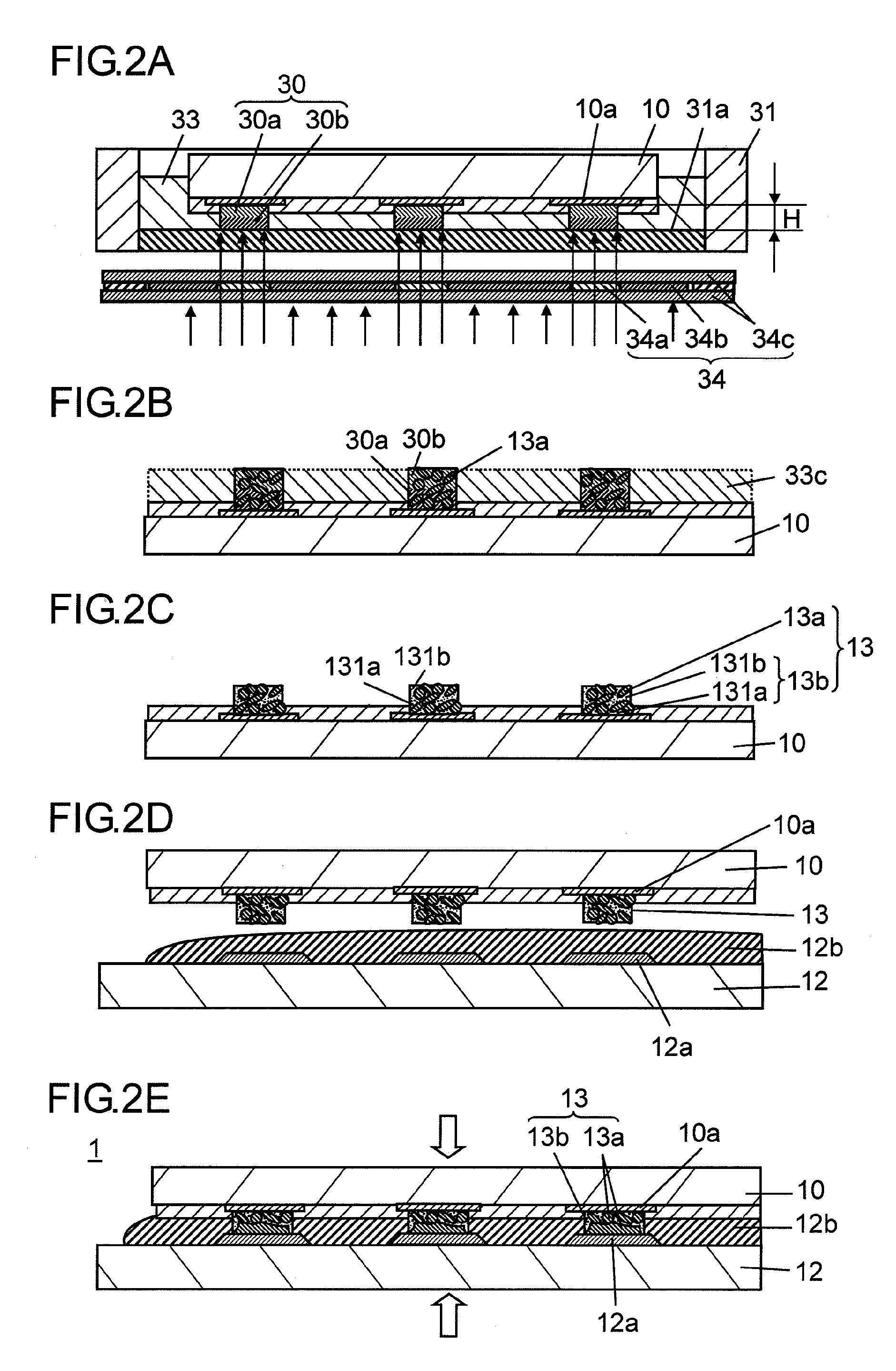
[0188]FIG. 7A to FIG. 7C are conceptual cross-sectional views showing the manufacturing method for electronic component mounting structure in the third preferred embodiment of the present invention. Same component elements as in the second preferred embodiment are given same reference marks in the description.
[0189]That is, the third preferred embodiment is different from the second preferred embodiment in such point that the protrusion electrode is formed while immersing the electronic component in the photosensitive resin liquid.
[0190]First, as shown in FIG. 7A, for example, photosensitive resin liquid 33 formed from photosensitive epoxy resin liquid, including conductive filler (not shown) such as 90% by weight of Sn—Ag—In solder alloy particles, is fed into container 71. And, electrode terminal 10a of electronic component 10 disposed at a stage (not shown) is immersed in photosensitive resin liquid 33 up to a position of predetermined interval t1 from the liquid surface of photo...
PUM
Abstract
Electronic component mounting structure (1) comprising electronic component (10) provided with a plurality of electrode terminals (10a), mounting substrate (12) provided with connector terminals (12a) in positions corresponding to electrode terminals (10a), wherein electrode terminal (10a) is connected to connector terminal (12a) via protrusion electrode (13) disposed on electrode terminal (10a) or connector terminal (12a), and protrusion electrode (13) includes at least conductive filler (13a) and photosensitive resin (13b), and varies in resin component crosslink density of photosensitive resin (13b) in the height direction of protrusion electrode (13).
Description
TECHNICAL FIELD[0001]The present invention relates to an electronic component mounting structure with an electronic component and a mounting substrate, and its manufacturing method.BACKGROUND ART[0002]With a recent trend of mobile equipment increasingly becoming higher in performance and smaller in size, electronic circuit devices are required to be larger in memory capacity, higher in performance, and smaller in size. Accordingly, there is a strong demand for high-density mounting based on finer and narrower pitch wiring rules for semiconductor elements.[0003]Conventionally, flip-chip mounting technology is available as a technology for high-density mounting of electronic components such as semiconductor elements on various wiring boards.[0004]In ordinary flip-chip mounting, for example, a solder bump of about 100 μm in diameter is formed on an electrode terminal of a semiconductor element such as LSI. After that, the semiconductor element is press-fitted and heated to connect the ...
Claims
Application Information
Patent Timeline
Application Date:The date an application was filed.
Publication Date:The date a patent or application was officially published.
First Publication Date:The earliest publication date of a patent with the same application number.
Issue Date:Publication date of the patent grant document.
PCT Entry Date:The Entry date of PCT National Phase.
Estimated Expiry Date:The statutory expiry date of a patent right according to the Patent Law, and it is the longest term of protection that the patent right can achieve without the termination of the patent right due to other reasons(Term extension factor has been taken into account ).
Invalid Date:Actual expiry date is based on effective date or publication date of legal transaction data of invalid patent.

