Semiconductor device

a semiconductor and memory system technology, applied in the field of semiconductor memory systems, can solve the problems of inability to achieve high-speed performance, inability to achieve sufficient display, and inability to process, etc., to achieve data writing/rewriting with small variance or no fluctuation, and low power consumption of the controller.

Inactive Publication Date: 2010-03-04
HITACHI LTD
View PDF10 Cites 24 Cited by
  • Summary
  • Abstract
  • Description
  • Claims
  • Application Information

AI Technical Summary

Benefits of technology

[0020]. . . as the number of rewriting operations becomes larger, the setting (to low-resistance state) becomes easier
[0021]An object of this invention is to provide a memory system which can solve the problems with the conventional art, and perform a stable operation by dealing with variances or fluctuations.
[0023]Similarly, in the case of a DVD-RAM based on a phase change as a storage principle, trial writing has conventionally been executed in a trial writing-only area. However, in a semiconductor phase-change memory, when a system of trial writing in a trial writing-only area is employed, it is important to deal with an easy increase in difference in number of executed writing operations between the memory area and the re-write area.
[0024]This invention has been developed in view of the aforementioned problems. An object of this invention is to provide a technology for realizing data writing / rewriting with small variance or no fluctuation in a data memory area by trial writing, and low power consumption of a controller.
[0027]The embodiment of this invention improves a yield of a memory element, a memory device or a memory system, and greatly reduces the cycle of verify-readings or eliminates verification. Thus, an effective data transfer speed can be increased. Low power consumption can be realized. Moreover, operation conditions are optimized as occasion demands during use by a user, and hence a highly reliable memory system can be built.

Problems solved by technology

Prechecking characteristics of the memory elements enables rewriting under optimal conditions as described in JP 2005-050424 A. However, this process is not practical, because it takes an extremely long period of time, and the memory is used for storing optimal conditions different from one element to another.
Thus, the cycle of verify-readings may be increased, disabling sufficient exhibition of high-speed performance.

Method used


Image

  • Semiconductor device
  • Semiconductor device
  • Semiconductor device

Examples


first embodiment

[0046]A first embodiment is directed to a configuration and a method for performing writing in a predetermined area of a memory array to optimize writing conditions when power is turned ON for a phase-change memory.

[0047]Overall System Configuration

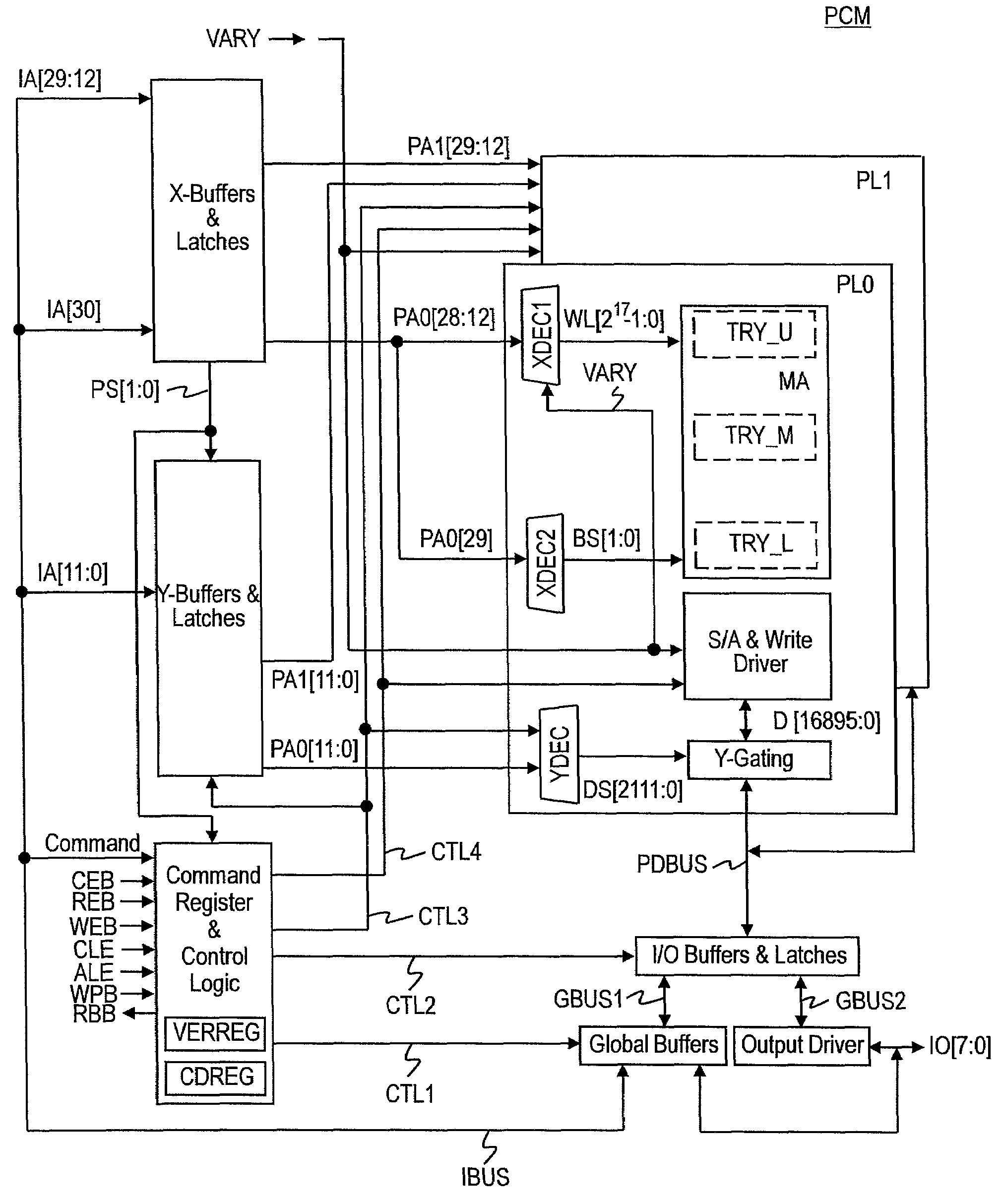
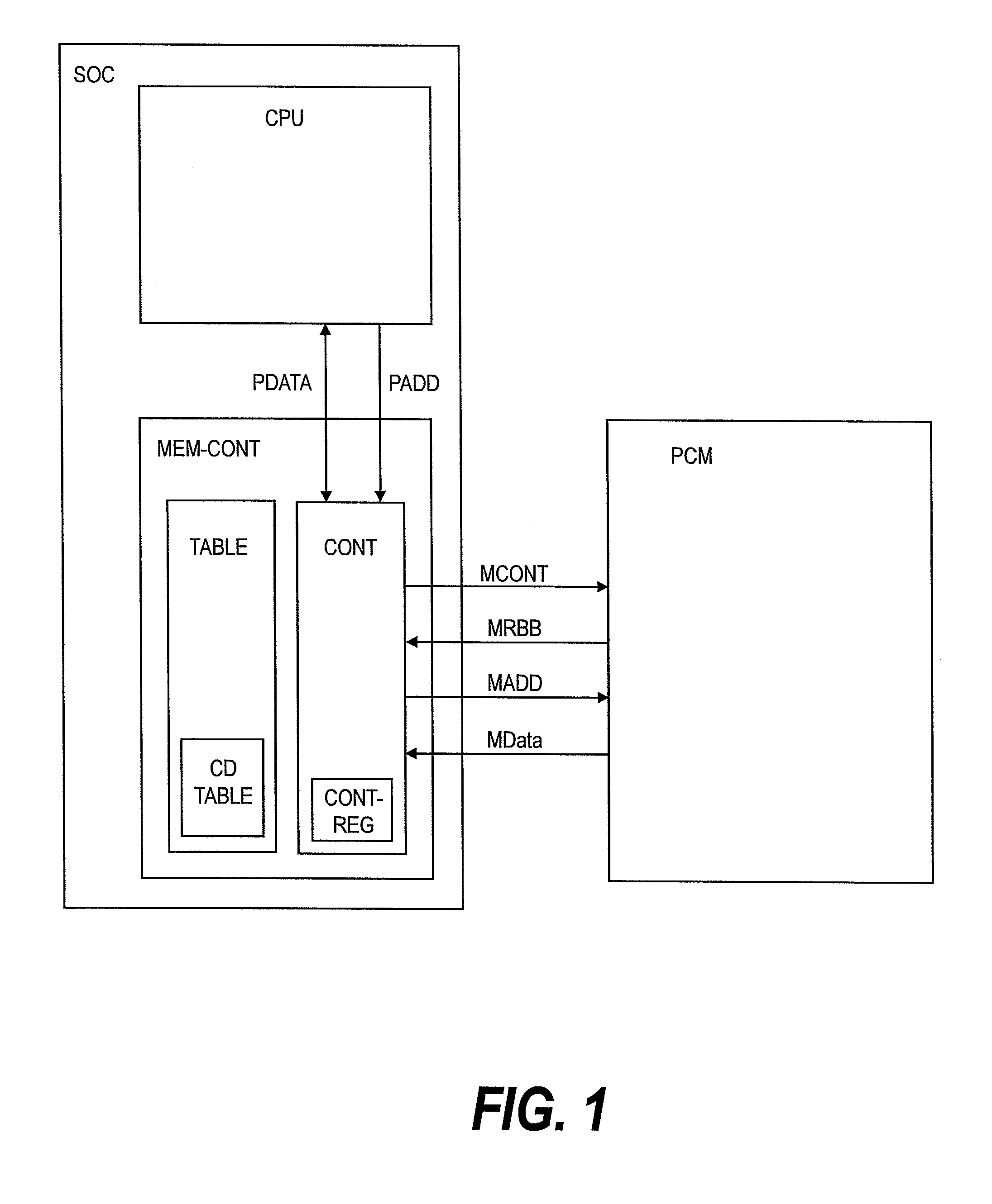
[0048]FIG. 1 illustrates an entire system of a semiconductor device according to the first embodiment of this invention. The system of this embodiment includes a central processing unit CPU, a phase-change memory PCM, and a memory controller MEM-CONT for receiving an instruction from the central processing unit CPU to control the phase-change memory PCM. The central processing unit CPU and the memory controller MEM-CONT are formed on the same semiconductor chip SOC. The memory controller MEM-CONT includes a management table TABLE and a control register CONT-REG. The management table TABLE includes a condition table CDTABLE. The central processing unit CPU and the phase-change memory PCM are coupled to each other via an address bus PADD an...

second embodiment

[0087]Next, a second embodiment of this invention is described. A phase-change system of the second embodiment includes an address replace circuit REP in a memory controller MEM_CONT as illustrated in FIG. 11. The address replace circuit REP checks whether writing fails when the writing is performed in a phase-change memory PCM. When the writing fails, the address replace circuit REP manages the address as a defect address, and manages which address the defect address is converted into. The address replace circuit REP registers a defect address identified by testing during manufacturing and its replace address.

[0088]In a phase-change element, even in the case of writing inhibition during manufacturing, in other words, a failure memory cell, applying writing currents several times may change element characteristics to enlarge a resistance change, in other words, to enable a normal operation. This embodiment is characterized in that by using such characteristics, writing is performed ...

third embodiment

[0092]A third embodiment of this invention is described. A configuration of a memory system of the third embodiment illustrated in FIG. 13 is different from that of the first embodiment illustrated in FIG. 1 in that a memory controller MEM_CONT includes a thermometer TMP. A phase-change memory PCM is easily affected by an ambient temperature because a state of a phase-change element is changed by a supplied amount of heat. In other words, a change in ambient temperature changes optimal writing conditions. In this embodiment, the ambient temperature is observed by the thermometer TMP, and when a change in ambient temperature is detected, a controller CONT is notified of the change by the thermometer TMP. The controller CONT that has received the notification performs a trial write operation similar to that of the first embodiment to set optimal conditions again.

[0093]In this way, even during an operation of the system, the optimal writing conditions can be maintained.

[0094]In this em...


PUM


Abstract

To realize a fast and highly reliable phase-change memory system of low power consumption, a semiconductor device includes: a memory device which includes a first memory array having a first area including a plurality of first memory cells and a second area including a plurality of second memory cells; a controller coupled to the memory device to issue a command to the memory device; and a condition table for storing a plurality of trial writing conditions. The controller performs trial writing in the plurality of second memory cells a plurality of times based on the plurality of trial writing conditions stored in the condition table, and determines writing conditions in the plurality of first memory cells based on a result of the trial writing. The memory device performs writing in the plurality of first memory cells based on the writing conditions instructed from the controller.

Description

CLAIM OF PRIORITY[0001]The present application claims priority from Japanese patent application JP2008-220785 filed on Aug. 29, 2008, the content of which is hereby incorporated by reference into this application.BACKGROUND OF THE INVENTION[0002]This invention relates to a semiconductor device, and more particularly, to a nonvolatile semiconductor memory system such as a phase-change memory or a phase-change random access memory (RRAM), and its controller.[0003]There are a phase-change memory and a phase-change optical disk as recording technologies which use physical properties of chalcogenide materials. As phase-change materials used therefor, chalcogenide materials including tellurium (Te) are known.[0004]U.S. Pat. No. 5,254,382 discloses an optical disk medium which uses, for a storage layer, a chalcogenide material represented by [(GeyTe1-y)a(SbzTe1-z)1-a]1-b(In1-xTex)b (in this case, 0.4≦y≦0.6, 0.3≦z≦0.6, 0.4≦z≦0.6, 0.1≦a≦0.5. 0.01≦b≦0.3). This chalcogenide material contains I...

Claims


Application Information

Patent Timeline
Patent Type & Authority Applications(United States)
IPC IPC(8): G06F11/26
CPCG11C13/0004G11C13/004G11C2213/72G11C13/0069G11C2013/0054G11C13/0064G11C29/028G11C29/50G11C29/50008G11C29/022
Inventor TERAO, MOTOYASUHANZAWA, SATORUKUME, HITOSHIOGUSHI, MINORUSASAGO, YOSHITAKAKINOSHITA, MASAHARUTAKAURA, NORIKATSU
Owner HITACHI LTD
Why Eureka
Try Eureka