

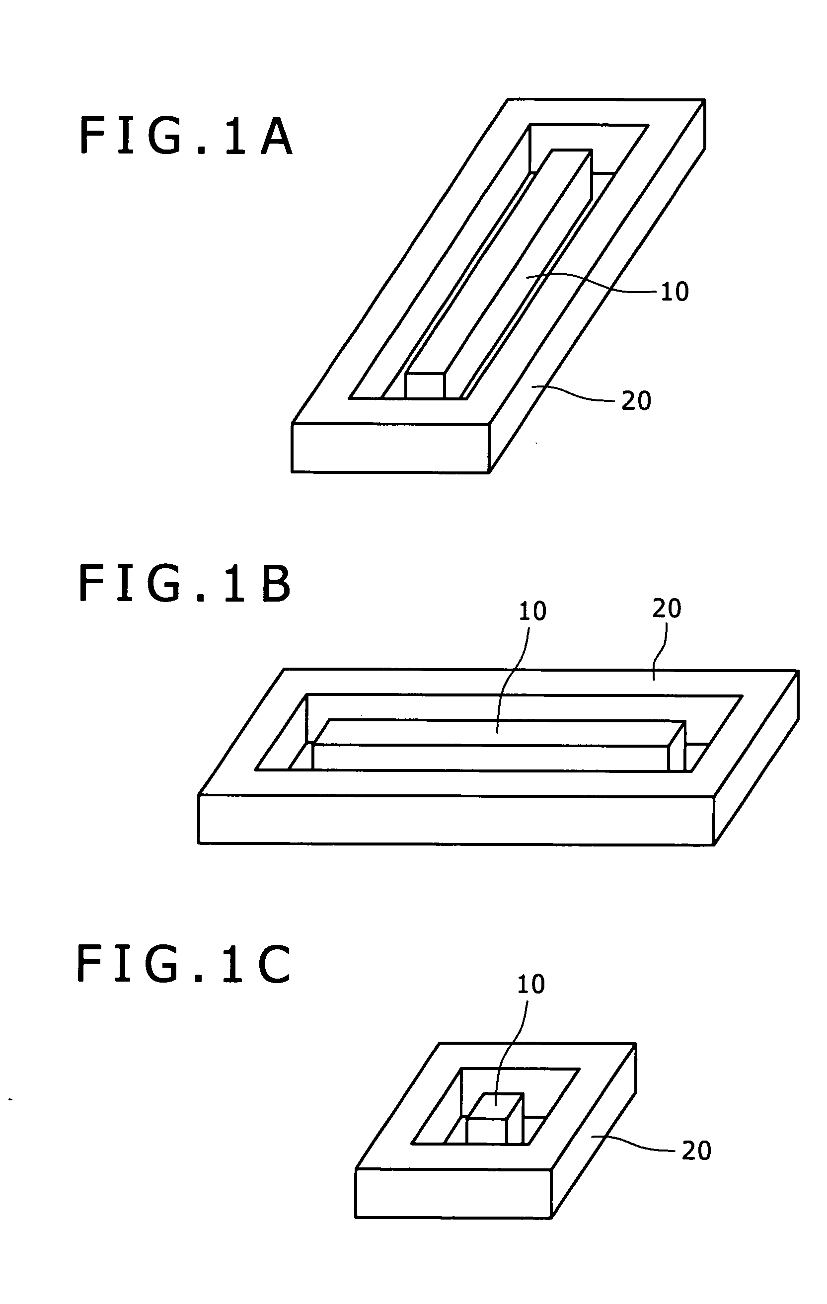
Capacitative element
a technology of capacitors and elements, applied in the field of capacitors, can solve the problems of loss of capacitance per unit area and bad influence exerted on the characteristics of analog circuits, and achieve the effect of sufficiently obtaining the capacitance per unit area and enhancing the shielding
- Summary
- Abstract
- Description
- Claims
- Application Information
AI Technical Summary
Benefits of technology
Problems solved by technology
Method used
Image

Examples
first embodiment
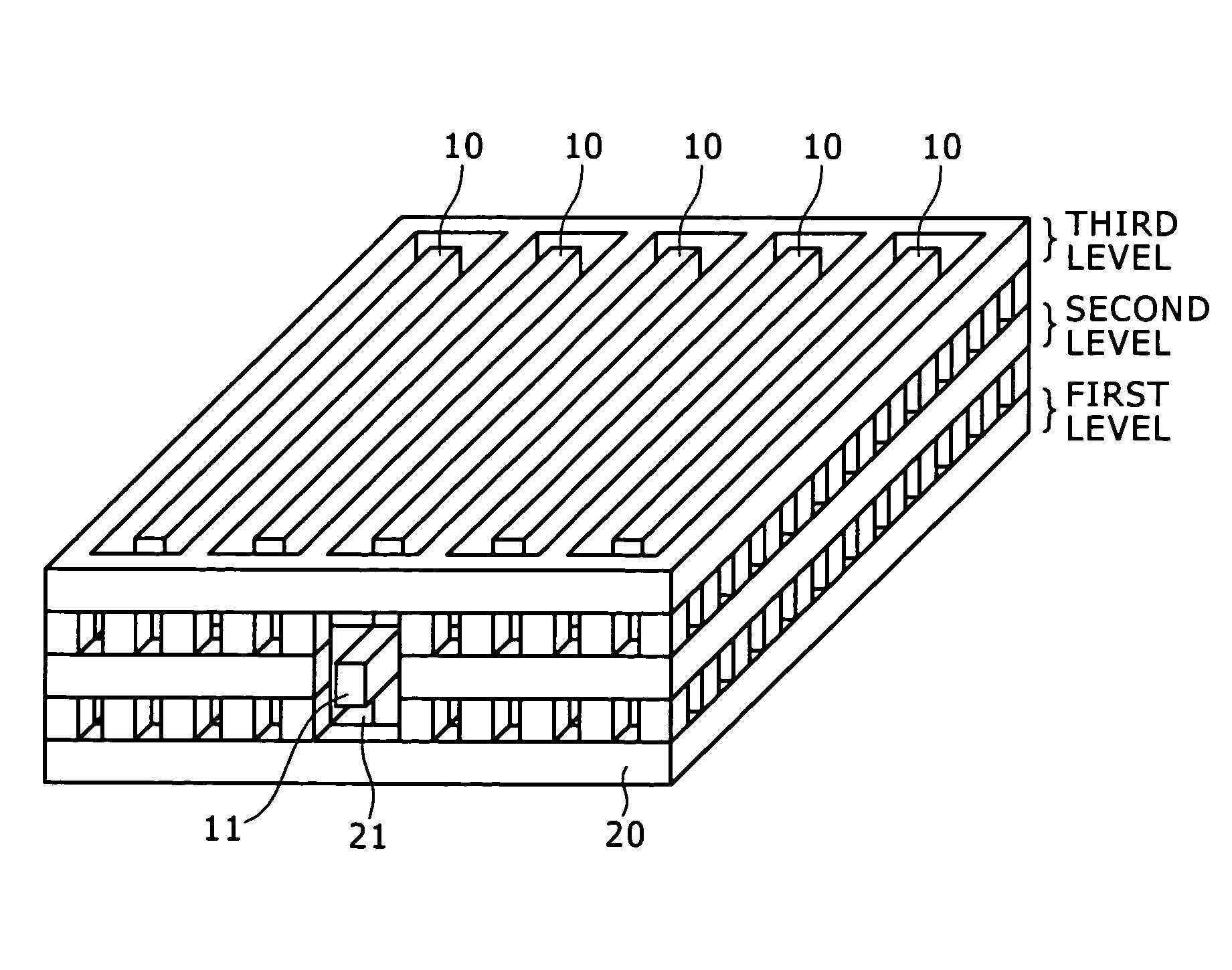
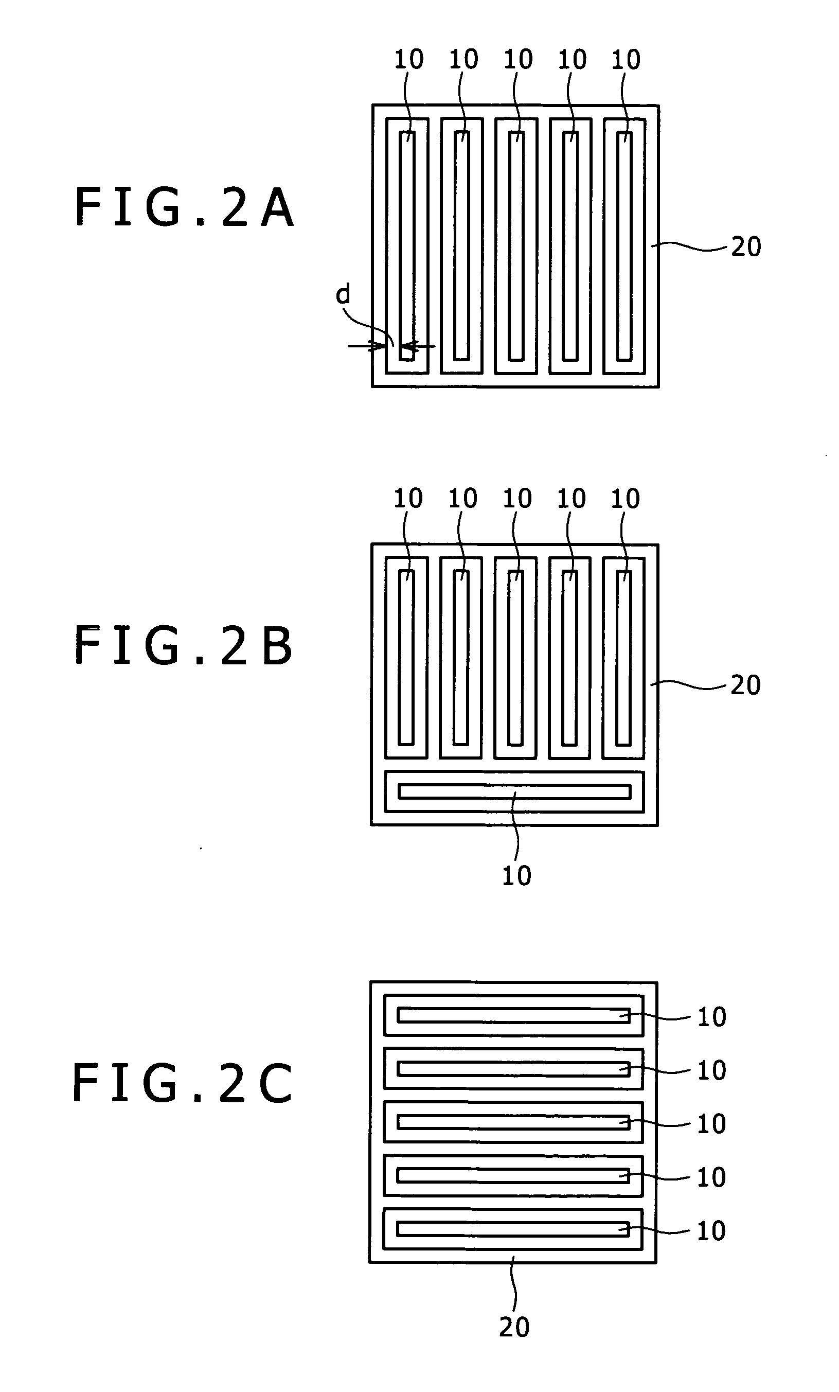
[0061]FIG. 6 is a perspective view showing a structure of a capacitative element according to a first embodiment of the present invention, and FIGS. 7A to 7C are respectively top plan views of first to third levels of the capacitative element of the first embodiment. Specifically, FIG. 7A shows a structure of the first level of the capacitative element of the first embodiment, FIG. 7B shows a structure of the second level of the capacitative element of the first embodiment, and FIG. 7C shows a structure of the third level of the capacitative element of the first embodiment. As shown in FIGS. 7A to 7C, each of the first electrodes 10 in the first level has a slender rod-like shape, and the second electrode 20 is formed so as to surround the first electrodes 10. This structure provides the unit capacitative element layer in which a plurality of unit capacitative elements each shown in any of FIGS. 1A to 1C are connected to one another along a surface of a semiconductor substrate (not ...
second embodiment
[0069]FIG. 8 is a perspective view showing a structure of a capacitative element according to a second embodiment of the present invention, and FIGS. 9A to 9C are respectively top plan views of first to third levels of the capacitative element of the second embodiment. Specifically, FIG. 9A shows a structure of the first level of the capacitative element of the second embodiment, FIG. 9B shows a structure of the second level of the capacitative element of the second embodiment, and FIG. 9C shows a structure of the third level of the capacitative element of the second embodiment. As shown in FIGS. 9A to 9C, each of the first electrodes 10 in the first level has a slender rod-like shape, and the second electrode 20 is formed so as to surround the first electrodes 10. This structure provides the unit capacitative element layer in which a plurality of unit capacitative elements each shown in any of FIGS. 1A to 1C are connected to one another along the surface of the semiconductor substr...
third embodiment
[0076]FIG. 10 is a perspective view showing a structure of a capacitative element according to a third embodiment, and FIGS. 11A to 11C are respectively top plan views of first to third levels of the capacitative element of the third embodiment. Specifically, FIG. 11A shows a structure of the first level of the capacitative element of the third embodiment, FIG. 11B shows a structure of the second level of the capacitative element of the third embodiment, and FIG. 11C shows a structure of the third level of the capacitative element of the third embodiment. As shown in FIGS. 11A to 11C, each of the first electrodes 10 in the first level has a slender rod-like shape, and the second electrode 20 are formed so as to surround the first electrodes 10. This structure provides the unit capacitative element layer in which a plurality of unit capacitative elements each shown in any of FIGS. 1A to 1C are connected to one another along the surface of the semiconductor substrate (not shown).
[0077...
PUM
 Abstract
Description
Claims
Application Information