Multi-pass programming for memory with reduced data storage requirement

a multi-pass programming and data storage technology, applied in the field of nonvolatile storage, can solve the problems of reducing the available separation between adjacent states and erroneous reading of stored data, and achieve the effect of reducing the coupling

Active Publication Date: 2010-03-11
SANDISK TECH LLC
View PDF24 Cites 217 Cited by
  • Summary
  • Abstract
  • Description
  • Claims
  • Application Information

AI Technical Summary

Benefits of technology

[0016]A programming technique is provided for reducing the effects of coupling between adjacent floating gates in a cost effective manner.

Problems solved by technology

The coupling from adjacent memory cells can shift the apparent charge level being read a sufficient amount to lead to an erroneous reading of the data stored.
As memory cells continue to shrink in size, the natural programming and erase distributions of threshold voltages are expected to increase due to short channel effects, greater oxide thickness / coupling ratio variations and more channel dopant fluctuations, thereby reducing the available separation between adjacent states.

Method used


Image

  • Multi-pass programming for memory with reduced data storage requirement
  • Multi-pass programming for memory with reduced data storage requirement
  • Multi-pass programming for memory with reduced data storage requirement

Examples


Embodiment Construction

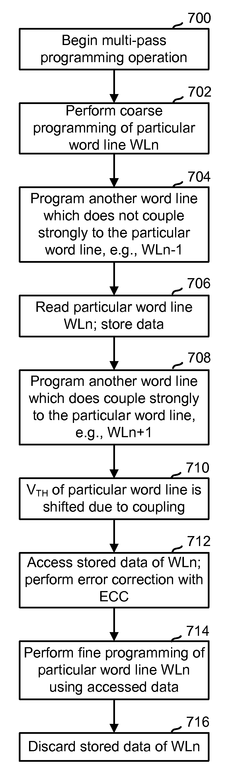
[0046]A programming technique is provided for reducing the effects of coupling between adjacent floating gates in a cost effective manner.

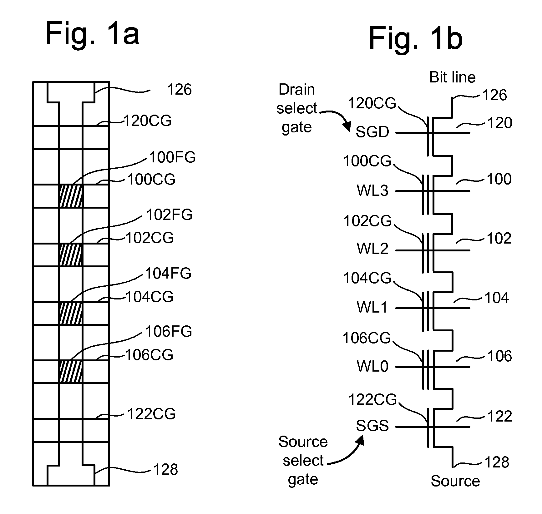
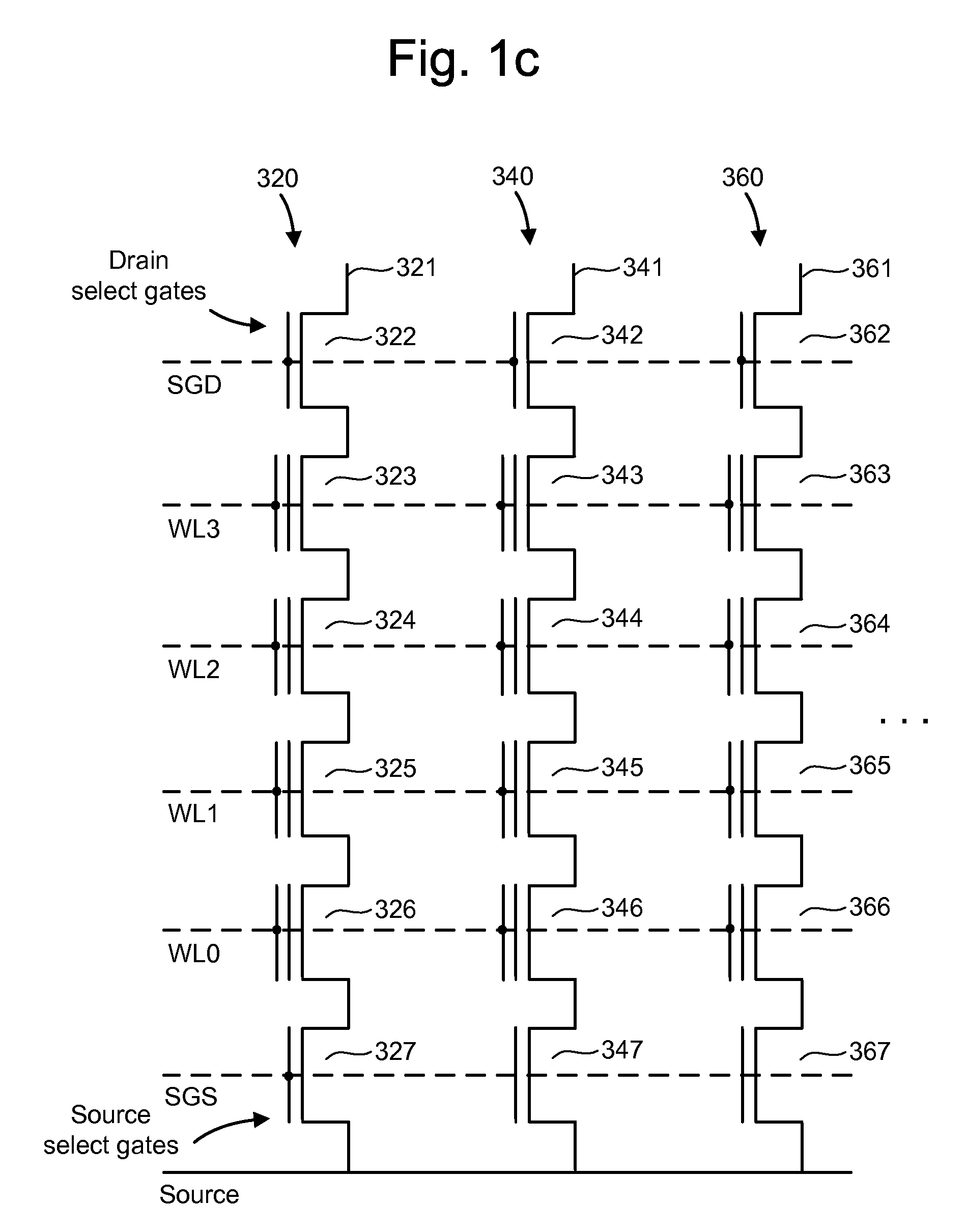
[0047]One example of a flash memory system uses the NAND structure, which includes arranging multiple transistors in series, sandwiched between two select gates. The transistors in series and the select gates are referred to as a NAND string. FIG. 1a is a top view showing one NAND string. FIG. 1b is an equivalent circuit thereof. The NAND string depicted in FIGS. 1a and 1b includes four transistors 100, 102, 104 and 106 in series and sandwiched between a first (drain side) select gate 120 and a second (source side) select gate 122. Select gate 120 connects the NAND string to a bit line via bit line contact 126. Select gate 122 connects the NAND string to source line 128. Select gate 120 is controlled by applying the appropriate voltages to select line SGD. Select gate 122 is controlled by applying the appropriate voltages to select line SGS. Each ...


PUM


Abstract

Coupling effects between adjacent floating gates in a non-volatile storage device are reduced in a multi-pass programming operation, while reducing program data storage requirements. In one approach, storage elements are programmed in an out of sequence or zigzag word line order. A particular word line is programmed with a coarse program pass, after which another word line is programmed with a fine program pass, after which the particular word line is read. The particular word line is read before another word line is programmed with a coarse program pass which causes coupling interference to storage elements of the particular word line. The read data is subsequently used to perform a fine program pass for the particular word line. This avoids the need to store program data of multiple word lines concurrently, so that storage hardware can be reduced in size along with power consumption.

Description

CROSS-REFERENCE TO RELATED APPLICATIONS[0001]This application claims the benefit of U.S. provisional patent application No. 61 / 096,221, filed Sep. 11, 2008, and incorporated herein by reference (docket no.: SAND-01378US1).BACKGROUND OF THE INVENTION[0002]1. Field of the Invention[0003]The present invention relates to technology for non-volatile storage.[0004]2. Description of the Related Art[0005]Semiconductor memory has become more popular for use in various electronic devices. For example, non-volatile semiconductor memory is used in cellular telephones, digital cameras, personal digital assistants, mobile computing devices, non-mobile computing devices and other devices. Electrical Erasable Programmable Read Only Memory (EEPROM) and flash memory are among the most popular non-volatile semiconductor memories.[0006]Both EEPROM and flash memory utilize a floating gate that is positioned above and insulated from a channel region in a semiconductor substrate. The floating gate is posi...

Claims


Application Information

Patent Timeline
Patent Type & Authority Applications(United States)
IPC IPC(8): G11C16/04G11C16/06
CPCG11C11/5628G11C2211/5621G11C16/3418
Inventor MIWA, TORUHEMINK, GERRIT JAN
Owner SANDISK TECH LLC
Why Eureka
Try Eureka