
Solar cells fabricated by using CVD epitaxial si films on metallurgical-grade si wafers

a technology of solar cells and epitaxial si films, applied in the field of solar cells, can solve the problems of high cost of conventional solar grade si, and high cost of solar cells to $3-$4 per watt peak

Active Publication Date: 2010-03-18
TESLA INC
View PDF5 Cites 42 Cited by
  • Summary
  • Abstract
  • Description
  • Claims
  • Application Information

AI Technical Summary

Problems solved by technology

The negative environmental impact caused by the use of fossil fuels and its rising cost have resulted in a dire need for cleaner, cheaper alternative energy sources.
However, the cost of conventional solar grade Si is well above $100 / kg, which drives the cost of solar cells to $3-$4 per Watt peak (Wp).
However, the quality of purified metallurgical Si wafers does not match that of solar-grade polysilicon, and the performance of the fabricated solar cell is less stable.
However, the multi-crystalline MG-Si substrate tends to produce multi-crystalline Si thin film, which results in a lower solar cell efficiency.
Although a high-performance solar cell is demonstrated, the cost of liquid phase growth is prohibitively high, thus hindering any possible commercial application.
However, the boron concentration in the Ciszek MG-Si substrate is too high to form a high-efficiency solar cell.

Method used


Image

  • Solar cells fabricated by using CVD epitaxial si films on metallurgical-grade si wafers
  • Solar cells fabricated by using CVD epitaxial si films on metallurgical-grade si wafers
  • Solar cells fabricated by using CVD epitaxial si films on metallurgical-grade si wafers

Examples


Embodiment Construction

[0026]The following description is presented to enable any person skilled in the art to make and use the invention, and is provided in the context of a particular application and its requirements. Various modifications to the disclosed embodiments will be readily apparent to those skilled in the art, and the general principles defined herein may be applied to other embodiments and applications without departing from the spirit and scope of the present invention. Thus, the present invention is not limited to the embodiments shown, but is to be accorded the widest scope consistent with the claims.

Overview

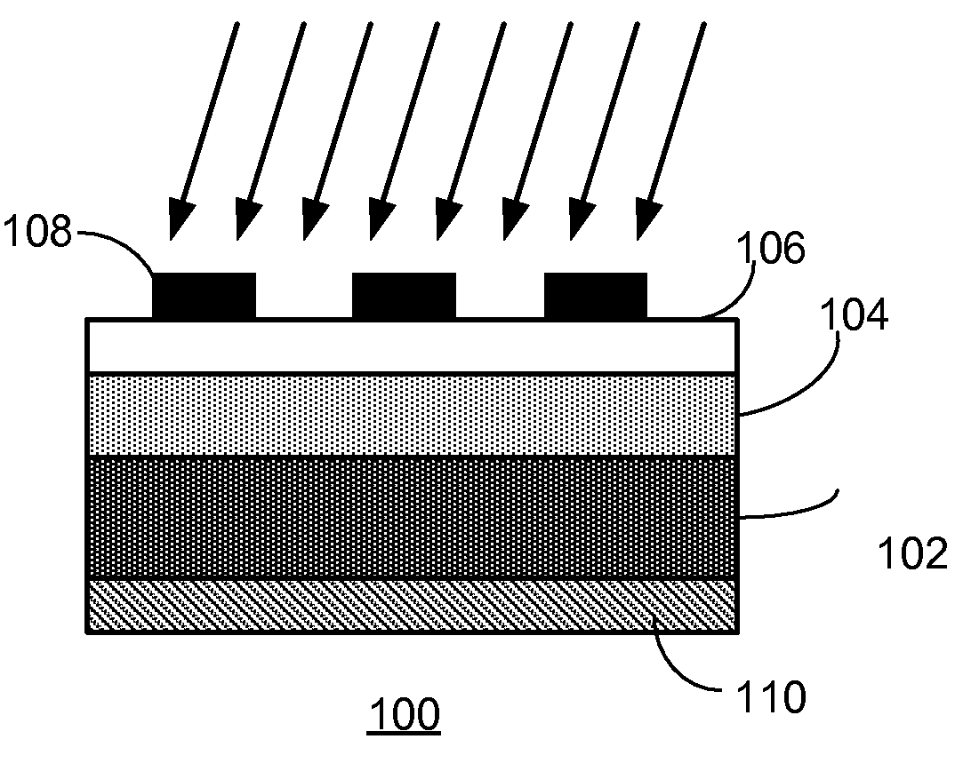
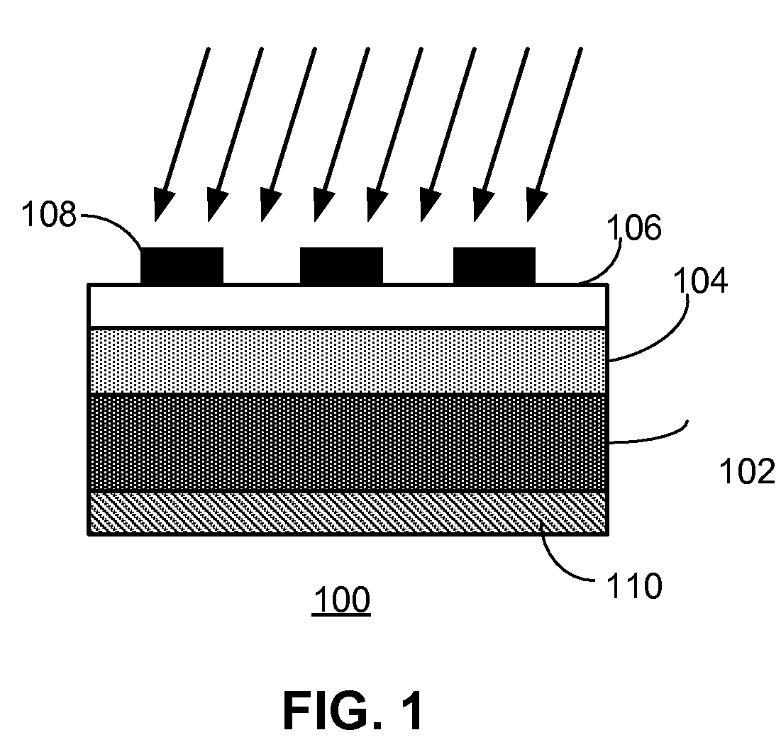
[0027]Embodiments of the present invention provide a solar cell based on epitaxial growth of single-crystal Si thin film on an MG-Si substrate. In one embodiment, an MG-Si substrate is obtained from an ingot grown using the Czochralski method. The MG-Si substrate is further leached out of metal impurities. A single-crystal Si thin film is grown on top of the MG-Si substrate using a CV...


PUM


Abstract

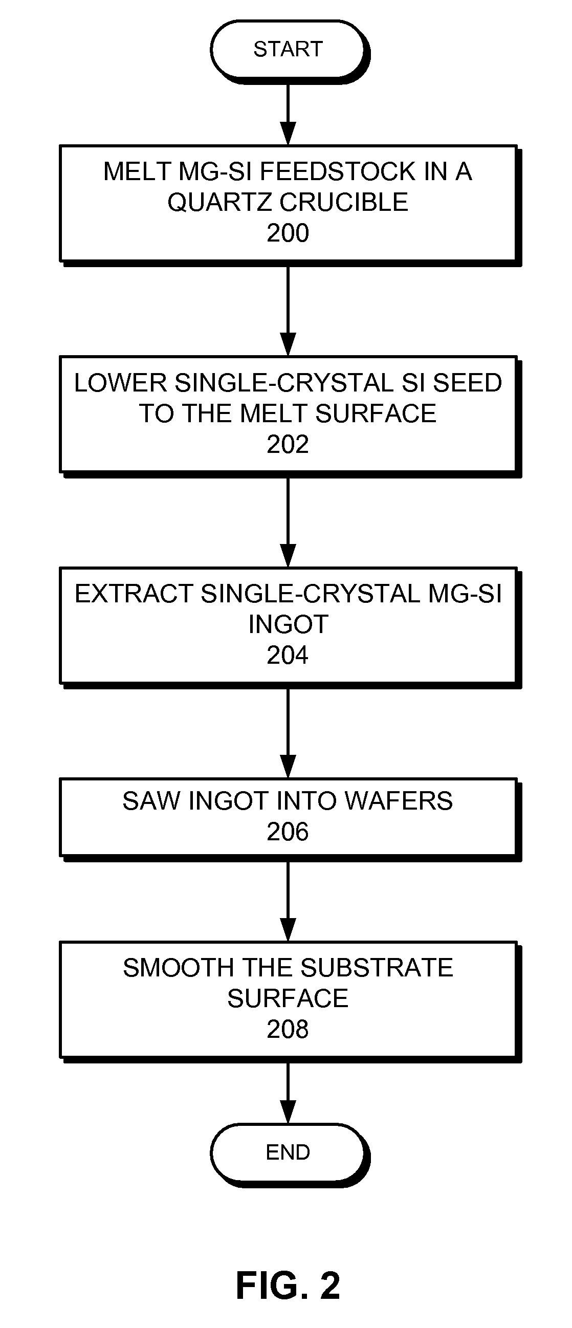
One embodiment of the present invention provides a method for fabricating a solar cell. The method includes: melting a metallurgical-grade (MG) Si feedstock, lowering a single-crystalline Si seed to touch the surface of the molten MG-Si, slowly pulling out a single-crystal Si ingot of the molten MG-Si, processing the Si ingot into single crystal Si wafers to form MG-Si substrates for subsequent epitaxial growth, leaching out residual metal impurities in the MG-Si substrate, epitaxially growing a layer of single-crystal Si thin film doped with boron on the MG-Si substrate, doping phosphor to the single-crystal Si thin film to form an emitter layer, depositing an anti-reflection layer on top of the single-crystal Si thin film, and forming the front and the back electrical contacts.

Description

RELATED APPLICATION [0001]This application claims the benefit of U.S. Provisional Application No. 61 / 097,471, Attorney Docket Number SSP08-1002PSP, entitled “Solar Cells Fabricated by Using CVD Epitaxial Si Films on Metallurgical-Grade Si Wafers” by inventors Jianming Fu, Zheng Xu, Peijun Ding, Chentao Yu, Guanghua Song, and Jianjun Liang, filed 16 Sep. 2008, and U.S. Provisional Application No. 61 / 102,228, Attorney Docket Number SSP08-1002PSP2, entitled “Solar Cells Fabricated by Using CVD Epitaxial Si Films on Metallurgical-Grade Si Wafers” by inventors Jianming Fu, Zheng Xu, Peijun Ding, Chentao Yu, Guanghua Song, and Jianjun Liang, filed 2 Oct. 2008.BACKGROUND[0002]1. Field of the Invention[0003]The present invention relates to solar cells. More specifically, the present invention relates to solar cells fabricated using CVD epitaxial Si films on metallurgical-grade (MG) Si wafers.[0004]2. Related Art[0005]The negative environmental impact caused by the use of fossil fuels and it...

Claims


Application Information

Patent Timeline
IPC IPC(8): H01L31/0288H01L31/068
CPCH01L31/068H01L21/3221Y02E10/547H01L31/1804Y02P70/50
Inventor FU, JIANMINGXU, ZHENGDING, PEIJUNYU, CHENTAOSONG, GUANGHUALIANG, JIANJUN
Owner TESLA INC
Learn More