Method and system for printing on a printed circuit board

a printed circuit board and printing system technology, applied in the field of methods and systems for printing on printed circuit boards, can solve the problems of short circuits by bridging solder, and achieve the effects of reducing board handling, saving valuable time, and improving deposition accuracy and reliability

Inactive Publication Date: 2010-03-18
CAMTEK LTD
View PDF4 Cites 14 Cited by
  • Summary
  • Abstract
  • Description
  • Claims
  • Application Information

AI Technical Summary

Benefits of technology

[0014]In accordance with these and other objects of the invention, the deposition of solder mask and the deposition of notation ink are combined within a single machine performing both processes. The combination of these two steps reduces board handling and improves accuracy of deposition as well as reliability. Curing can be combined for the two steps and be performed at once, thus saving valuable time.

Problems solved by technology

The solder resist mask leaves uncovered only the pads that need to be covered by the molten solder; otherwise, the conducting paths would also be covered with solder, causing several problems such as short circuits by bridging solder.

Method used


Image

  • Method and system for printing on a printed circuit board
  • Method and system for printing on a printed circuit board
  • Method and system for printing on a printed circuit board

Examples


Embodiment Construction

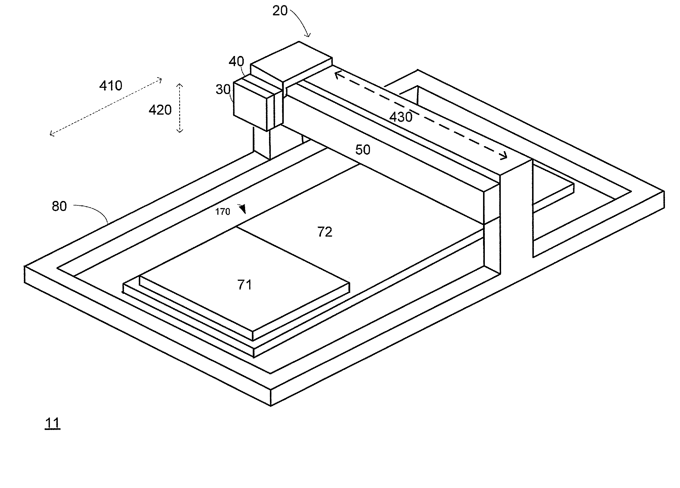
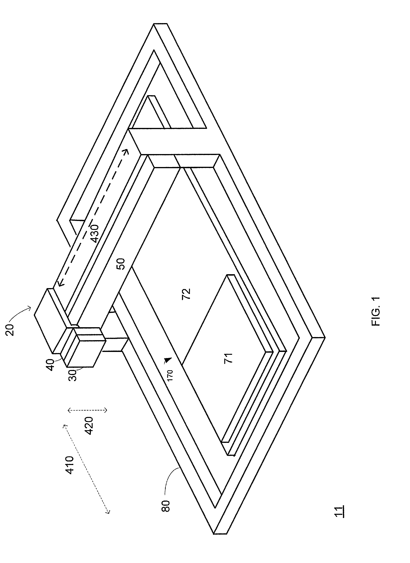
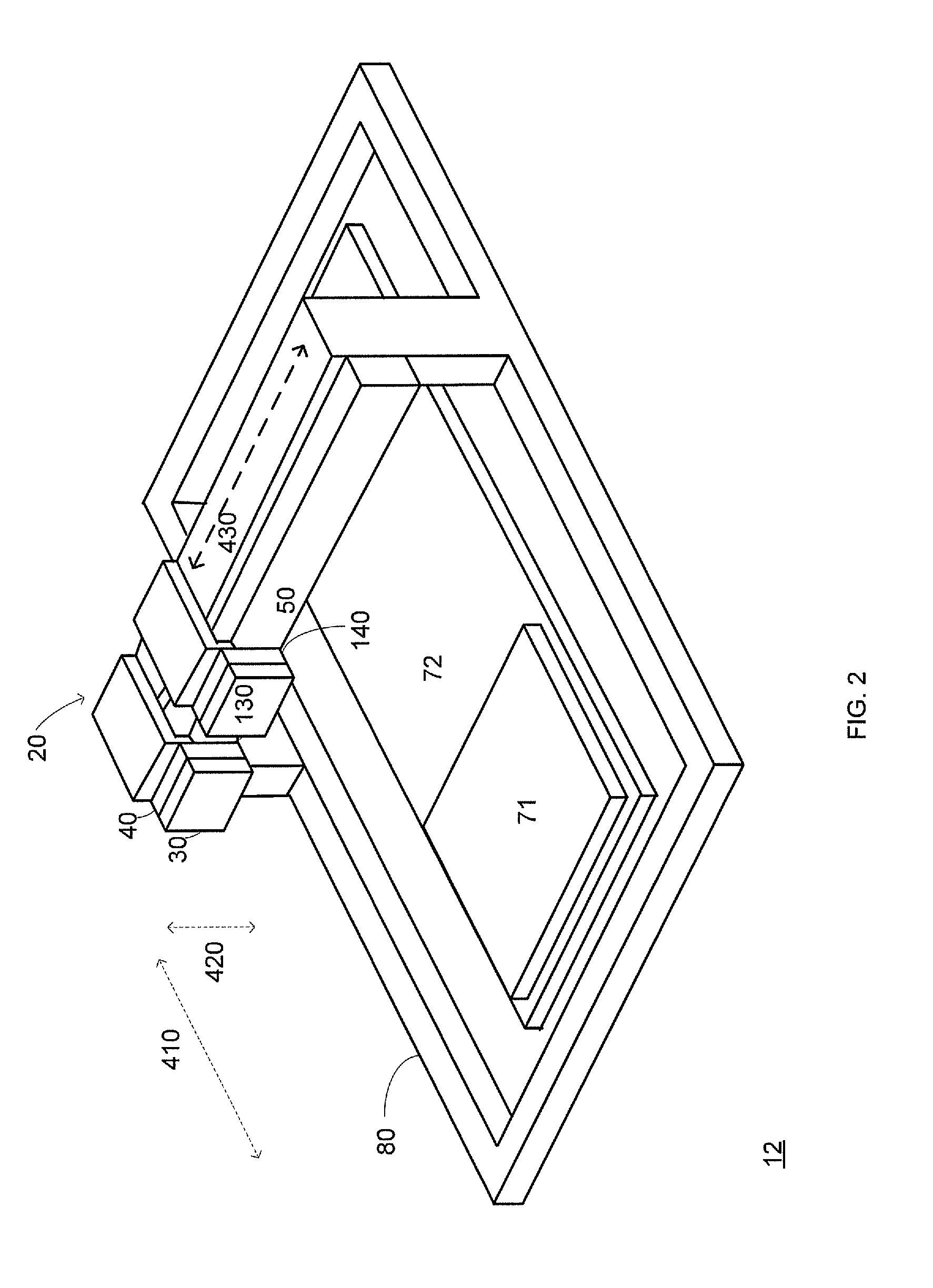
[0033]In the following detailed description, numerous specific details are set forth in order to provide a thorough understanding of the invention. For convenience of explanation, the invention is described below with reference to preferred embodiments, which comprise a legend printing and a solder mask printing system. However, it will be understood by those of ordinary skill in the art that the present invention may be practiced without these specific details. For example, those versed in the art will readily appreciate that the invention is by no means bound to these embodiments and various dispensing methods for, inter alia, primary image conducting patterns, etch resist mask patterns, temporary masks, edging non-uniformity compensation control masks, selective conformal coatings, chip-on-board encapsulation, liquid encapsulates, bar codes, and adhesives in surface mount technology (SMT), are within the scope of the present invention. Furthermore, applying certain minor modifica...


PUM


Abstract

A method, a printing system and a printing bridge. The printing bridge is configured to accommodate in a precise manner a jet print head. The jet print head includes first jet nozzles for injecting a first type jettable substance to form a first pattern onto the surface of a object, and a second jet nozzles for injecting a second type of jettable substance to form a first pattern onto the surface of a object. The first type jettable substance is utilized for printing a solder mask pattern and the second type jettable substance is utilized for printing a legend pattern.

Description

RELATED APPLICATIONS[0001]This application is a continuation in part of U.S. patent application Ser. No. 11 / 907,346 titled “Method and apparatus for PCB finishing processes”, filing date Oct. 11, 2007.FIELD OF THE INVENTION[0002]The present invention relates to an apparatus combining various elements in the PCB finishing processes and a method for combining steps in the digital manufacturing of printed circuit boards (PCB) using inkjet printers.BACKGROUND OF THE INVENTION[0003]The printed circuit board (PCB) or printed wiring board (PWB) is the object that connects and interfaces most electronic components with each other and with other elements in computers, communication devices, consumer electronics, automated manufacturing and inspection equipment.[0004]The procedures of manufacturing these circuit boards and of inserting and connecting multiple components, such as resistors, capacitors and integrated circuits, can be applied in mass production environments, achieving substantia...

Claims


Application Information

Patent Timeline
Patent Type & Authority Applications(United States)
IPC IPC(8): B41J2/145
CPCB41J3/28B41J3/543H05K2203/013H05K3/0091H05K3/28H05K1/0266
Inventor YAFE, ALBERT
Owner CAMTEK LTD
Why Eureka
Try Eureka