Organic electroluminescence display device

a display device and organic technology, applied in the direction of discharge tube luminescnet screens, discharge tube/lamp details, electric discharge lamps, etc., can solve the problems of large mask distortion, difficult to make a mask design which takes distortion into account, and displacement of vapor deposition, so as to improve the degree of design freedom and improve the effect of vapor deposition accuracy

Active Publication Date: 2010-05-11
SAMSUNG DISPLAY CO LTD +1
View PDF3 Cites 2 Cited by
  • Summary
  • Abstract
  • Description
  • Claims
  • Application Information

AI Technical Summary

Benefits of technology

[0016]According to the present invention it is possible to improve the vapor deposition accuracy and improve the degree of design freedom.

Problems solved by technology

When a thermal stress is applied to the vapor deposition mask in a vapor deposition process, there occurs a fine deformation, causing a vapor deposition displacement.
In such a structure, not only there occurs a large distortion of the mask as the end portion, but also it is very difficult to make a mask design which takes distortion into account.
In the case where the mask end portion is square in shape, the stress is concentrated on two places, causing deterioration of the mask accuracy.

Method used


Image

  • Organic electroluminescence display device
  • Organic electroluminescence display device
  • Organic electroluminescence display device

Examples


first embodiment

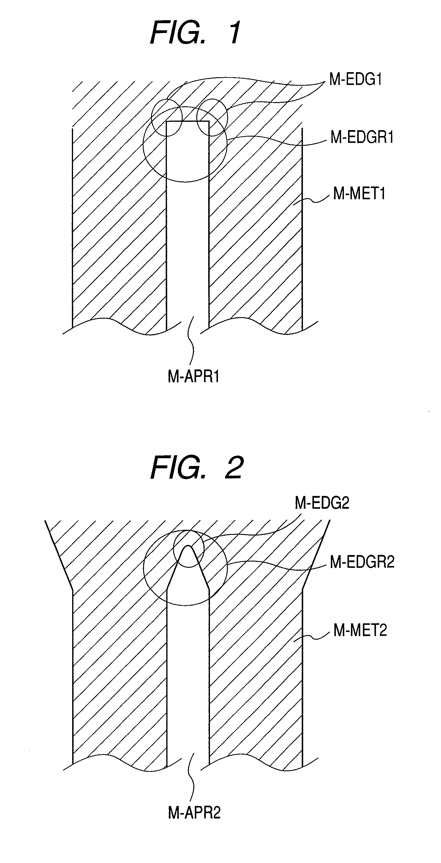
[0028]The shape of a vapor deposition mask according to the present invention is shown in FIG. 2. In this vapor deposition mask, the width of an end portion M-EDGR2 of a hole M-APR2 in a mask portion M-MET2 is gradually narrowed like an outwardly convex curved line and a vertex M-EDG2 thereof is rounded to disperse stress.

[0029]This shape can be designated a generally triangular shape having a round tip, but it is not always necessary that the end portion be curved or rounded. There may be adopted a structure wherein straight lines are connected in a continuous manner. However, a differentiable curved line is preferred. As to the type of this curved line, a curved line capable of being approximated to a conic section or a quadratic curve is preferred. A curved line capable of being approximated to an ellipse, a parabola or a hyperbola is more preferred. The most effective shape in comparison with a rectangular shape is a shape capable of being designated a generally triangular shape...

second embodiment

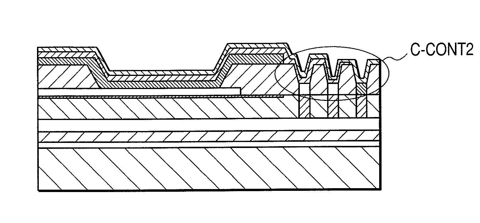
[0033]The following description is now provided about another structure of an organic EL display device which could be implemented by the using the vapor deposition mask of the first embodiment which made vapor deposition possible up to near the outside of the dummy pixel area. In case of forming a cathode metal into a film by the conventional vapor deposition method, the heat energy of metal particles is large because vapor deposition is performed at a very high temperature. It is presumed that when the metal particles adhere to a circuit board, there will occur a film stress due to a difference in temperature between the metal particles and the circuit board, with a consequent increase of contact resistance in the cathode contact portion. This increased contact resistance acts as an internal resistance of the organic EL display element, causing an increase of the organic EL display device driving voltage, and it has been one of factors of an increase in power consumption of the or...

third embodiment

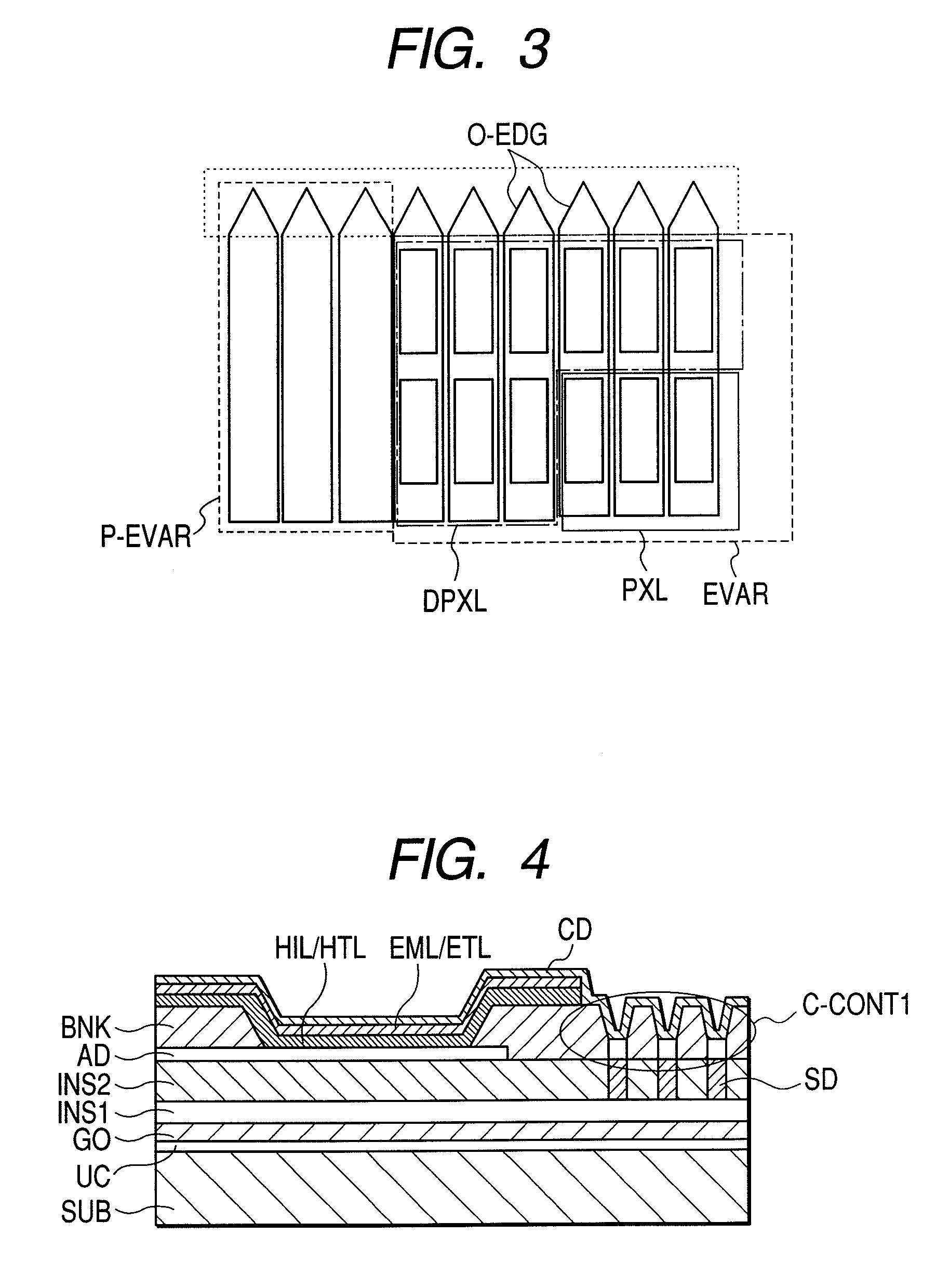
[0046]A vapor deposition area of an organic EL display device according to a third embodiment of the present invention is shown in FIG. 6. A different point from the second embodiment is that at each side a vapor deposition area of a luminescence layer EML and an electron transport layer ETL is wider than a vapor deposition area of a hole injection layer HIL and a hole transport layer HTL.

[0047]FIG. 7 is an enlarged diagram of a circled area, i.e., a left upper end portion of the pixel area, in FIG. 6. A double square area located on the right lower side is a display pixel area PXL. In the display pixel area PXL are disposed three pixels of RGB as one set. On upper, left and obliquely upper sides of those display pixels there is formed an organic EML like the display pixels. Dummy pixels of RGB with aperture not formed in the BNK are each arranged one set, i.e., a total of three sets. A hole injection layer HIL and a hole transport layer HTL are vapor-deposited as solid vapor deposi...


PUM


Abstract

An organic electroluminescence display device is disclosed wherein plural organic electroluminescence elements each having an anode, a cathode and an organic layer sandwiched in between the anode and the cathode, the plural organic electroluminescence elements including organic electroluminescence elements developing different colors in a row direction, and at least one of the organic layers having an outer edge of a conic section at an end portion in a column direction thereof, the outer edge of the conic section becoming narrower gradually in its width in a row direction of vapor deposition thereof toward an extreme end at an end portion in a column direction thereof. The organic electroluminescence display device can improve the vapor deposition accuracy and the degree of design freedom.

Description

CLAIM OF PRIORITY[0001]The present application claims priority from Japanese Application JP 2006-051282 filed on Feb. 27, 2006, the content of which is hereby incorporated by reference into this application.BACKGROUND OF THE INVENTION[0002](1) Field of the Invention[0003]The present invention relates to a vapor deposition area of an organic layer in an organic electroluminescence (EL) display device.[0004](2) Description of the Related Art[0005]As methods for forming a film of an organic layer of an organic EL display device there are known a printing method and a vapor deposition method. It is mainly the vapor deposition method that is practically applied to an organic EL display device using a low molecular organic material. Also as to an upper electrode, a film is formed mainly by vapor deposition.[0006]A laminate structure of a conventional organic film is composed of an anode electrode as a lower electrode, a hole injection layer, a hole transport layer, a light emitting layer,...

Claims


Application Information

Patent Timeline
Patent Type & Authority Patents(United States)
IPC IPC(8): H01J1/62
CPCH01L27/3223H01L51/56H01L51/5221H01L27/3279H01L27/3211H10K59/88H10K59/35H10K59/1315H10K50/82H10K71/00
Inventor MATSUDATE, NORIHARUOOKAWARA, TAKESHIKAJIYAMA, KENTA
Owner SAMSUNG DISPLAY CO LTD
Why Eureka
Try Eureka