Semiconductor Device and Manufacturing Method Thereof

Inactive Publication Date: 2010-03-25
SEMICON ENERGY LAB CO LTD
View PDF38 Cites 14 Cited by
  • Summary
  • Abstract
  • Description
  • Claims
  • Application Information

AI Technical Summary

Benefits of technology

[0006]Accordingly, an object of an embodiment of the present invention is to provide a resistor whose characteristic values can be changed without requiring a photolithography process again after the circuit is completed.

Problems solved by technology

This is complicated because a photolithography process is necessary again after the circuit is completed.

Method used


Image

  • Semiconductor Device and Manufacturing Method Thereof
  • Semiconductor Device and Manufacturing Method Thereof
  • Semiconductor Device and Manufacturing Method Thereof

Examples


embodiment 1

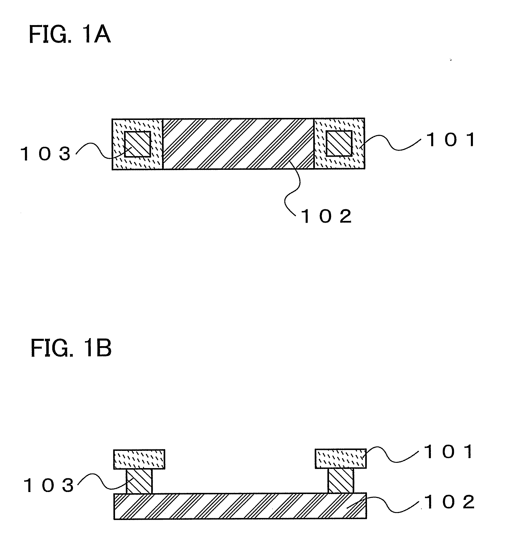
[0030]Embodiment 1 describes a structure of a resistor.

[0031]FIG. 1A is a top view of a resistor and FIG. 1B is a longitudinal sectional view thereof.

[0032]The resistor includes a metal layer 101 (a second conductive layer), a silicon layer 102 including amorphous silicon or polysilicon doped with an impurity (a first conductive layer), and a conductor 103 for connecting the metal layer 101 and the silicon layer 102 to each other.

[0033]The metal layer 101 can be formed from titanium, molybdenum, tungsten, aluminum, copper, silver, gold, nickel, platinum, palladium, iridium, rhodium, tantalum, cadmium, zinc, iron, or the like.

[0034]By setting as appropriate the condition of ion implantation, such as the kind, the amount, and the like of the impurity which is added to the silicon layer 102 of the resistor by doping, the resistor can have a desired resistance value.

[0035]As for the kind of impurity, in order to obtain silicon having n-type conductivity, an impurity including phosphorus...

embodiment 2

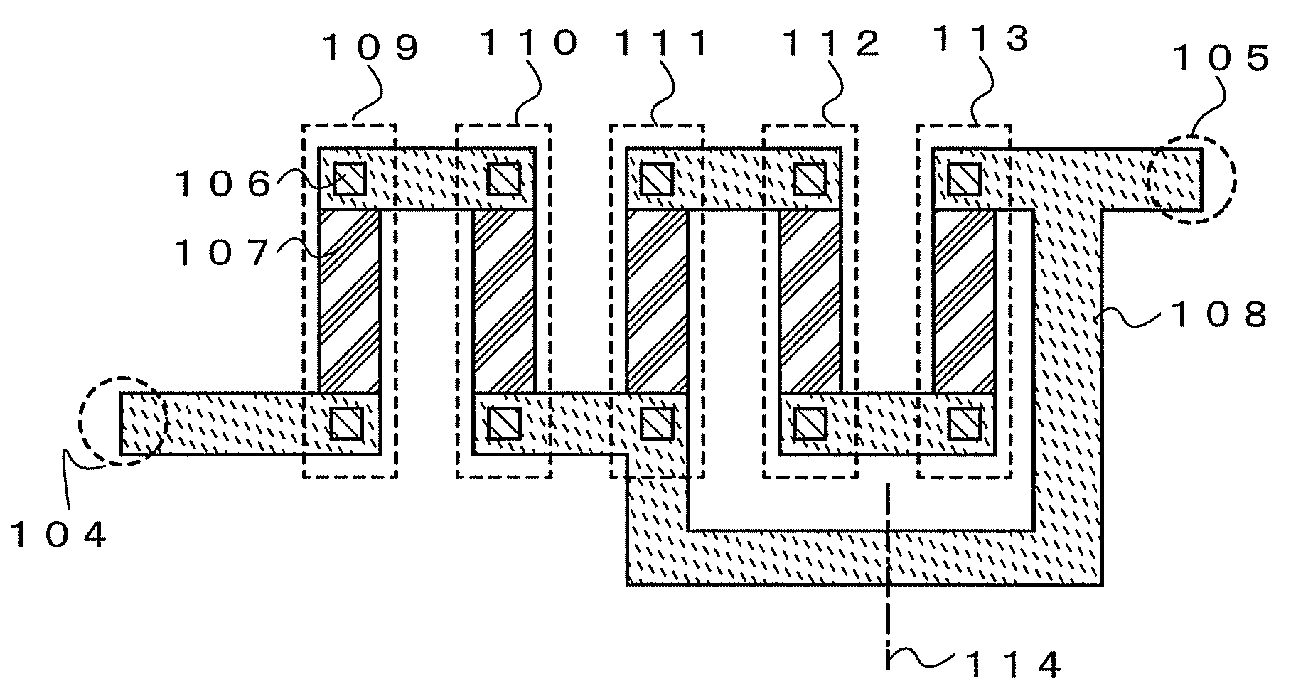
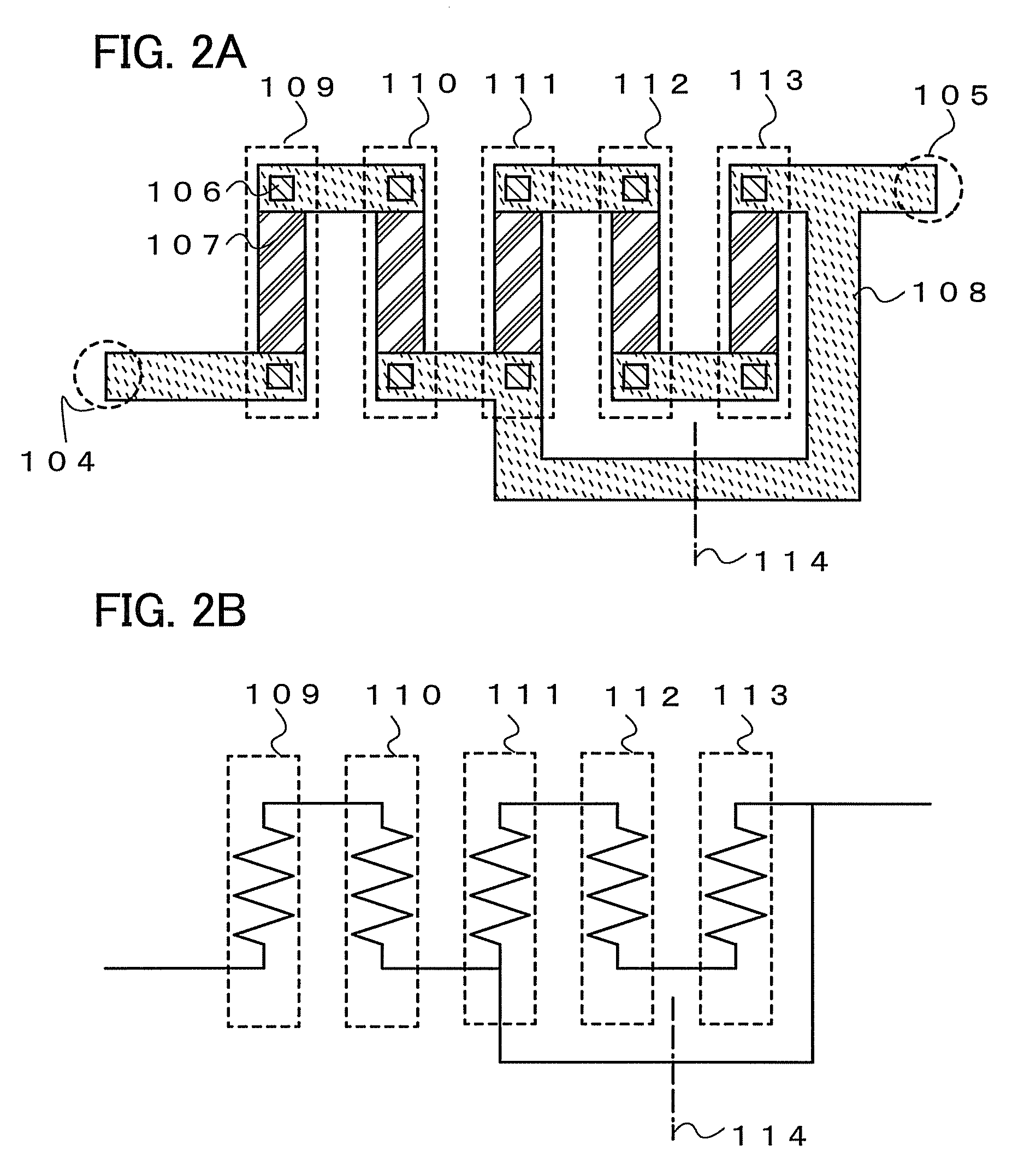
[0056]In FIG. 4A, a parallel resistor unit 116 includes resistors which are connected in parallel to each other, a parallel resistor unit 117 includes resistors which are connected in parallel to each other, and a parallel resistor unit 118 includes resistors which are connected in parallel to each other. The parallel resistor units 116, 117, and 118 are connected to each other with wirings to form a resistor element having a desired resistance value.

[0057]FIG. 4B is a circuit diagram of FIG. 4A.

[0058]Since the wiring has a much lower resistance value (or resistivity) than the resistor, the wiring is not regarded as a resistor.

[0059]The mask layout is designed as illustrated in FIG. 4A, and a process for manufacturing a semiconductor device is performed.

[0060]In evaluation, inspection, and the like after the completion of manufacture of the semiconductor device, in some cases, the resistance value (or resistivity) is deviated from the value set in the mask layout due to variation in...

embodiment 3

[0068]Embodiment 3 describes an example of a semiconductor device including the resistor of Embodiment 1 or Embodiment 2.

[0069]FIG. 6 illustrates one of a plurality of thin film transistors and one of the resistors of Embodiment 1 or Embodiment 2.

[0070]The semiconductor device illustrated in FIG. 6 includes a thin film transistor 302 in which a base insulating film 301, a semiconductor layer 302a, a gate insulating film 302b, and a gate electrode 302c are stacked over a substrate 300 in that order; a layer 303 including a resistor; an interlayer insulating film 304; and wirings 305a to 305d.

[0071]The base insulating film 301 is provided over the substrate 300, the thin film transistor 302 and the layer 303 including a resistor are provided over the base insulating film 301, the interlayer insulating film 304 is provided over the thin film transistor 302 and the layer 303 including a resistor, and the wirings 305a to 305d are provided over the interlayer insulating film 304.

[0072]As...


PUM


Abstract

A resistor whose characteristic value can be changed without requiring a photolithography process again is provided. The resistor includes a plurality of first resistor units which is connected serially to each other and a second resistor unit which is connected in parallel to part of the first resistor units. Then, after the measurement of a semiconductor integrated circuit, the second resistor unit is electrically disconnected as necessary. The first resistor units may be either a unit including a single resistor or may be a unit including a plurality of resistors.

Description

TECHNICAL FIELD[0001]The present invention relates to a resistor and a manufacturing method thereof, a semiconductor device and a manufacturing method thereof, and the like.BACKGROUND ART[0002]A semiconductor device provided with a semiconductor integrated circuit includes a switching element such as a TFT, a capacitor, a resistor, and the like.[0003]The characteristic values of a switching element, a capacitor, and a resistor are determined when they are designed, and usually cannot be changed after the semiconductor integrated circuit is completed.[0004]In view of the above, a technique is disclosed by which a spare element group formed in advance is used for modifying the characteristics of a semiconductor integrated circuit in accordance with the evaluation on the characteristics (Patent Document 1).[Patent Document 1] Japanese Published Patent Application No. 11-251529DISCLOSURE OF INVENTION[0005]According to the technique disclosed in Patent Document 1, masks for wirings and c...

Claims


Application Information

Patent Timeline
Patent Type & Authority Applications(United States)
IPC IPC(8): H01L29/86H01L21/02
CPCH01C1/16H01C13/02H01L23/5228H01L2924/12044H01L28/20H01L28/24H01L23/5258H01L2924/0002H01L2924/00
Inventor OHSHIMA, KAZUAKI
Owner SEMICON ENERGY LAB CO LTD
Why Eureka
Try Eureka