Solid-state imaging device, method of manufacturing the same, and electronic apparatus

a technology of solid-state imaging and manufacturing methods, applied in the direction of color television, television systems, radio control devices, etc., can solve the problems of difficult to form waveguides and difficult to maintain optical properties, and achieve the effects of improving imaging characteristics, improving imaging characteristics, and improving imaging characteristics

Inactive Publication Date: 2010-04-01
SONY SEMICON SOLUTIONS CORP
View PDF2 Cites 23 Cited by
  • Summary
  • Abstract
  • Description
  • Claims
  • Application Information

AI Technical Summary

Benefits of technology

[0024]In the waveguide having the highly symmetrical structure at positions located at a certain height from the surface of the substrate both in the cross-section taken along the line XXVIII-XXVIII (in the horizontal direction) and in the cross-section taken along the line XXIX-XXIX (in the vertical direction) as described above, the following problem easily occurs. That is, in the waveguide, incoming light and light totally reflected with phases shifted with respect to each other easily interfere with each other, standing waves are easily generated, and phases of light incident on the photodiode (PD) are easily aligned.
[0043]In the electronic apparatus according to the other embodiment of the present invention, since the occurrence of spectral ripples is suppressed and imaging characteristics are improved in the solid-state imaging device, quality improvement can be achieved.

Problems solved by technology

In solid-state imaging devices, in particular, in CCD solid-state imaging devices, with a decrease in the pixel cell size, it has become difficult to maintain optical properties, such as sensitivity and an anti-smear property.
Furthermore, it is difficult to form waveguides by self-alignment with respect to the transfer electrodes and the connecting conductive layers, and it is necessary to control the process margin, such as the misalignment of the mask.

Method used


Image

  • Solid-state imaging device, method of manufacturing the same, and electronic apparatus
  • Solid-state imaging device, method of manufacturing the same, and electronic apparatus
  • Solid-state imaging device, method of manufacturing the same, and electronic apparatus

Examples


first embodiment

1. First Embodiment

Example of Structure of Solid-State Imaging Device

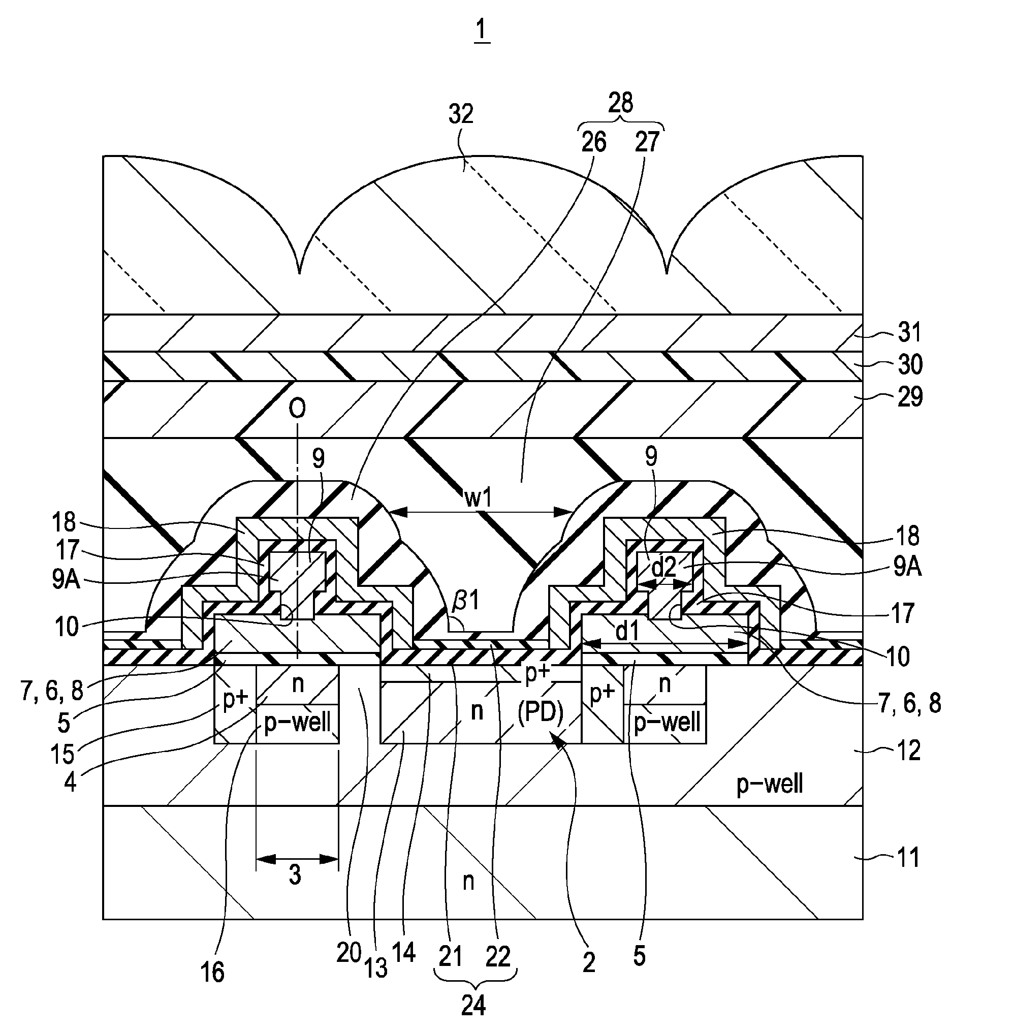
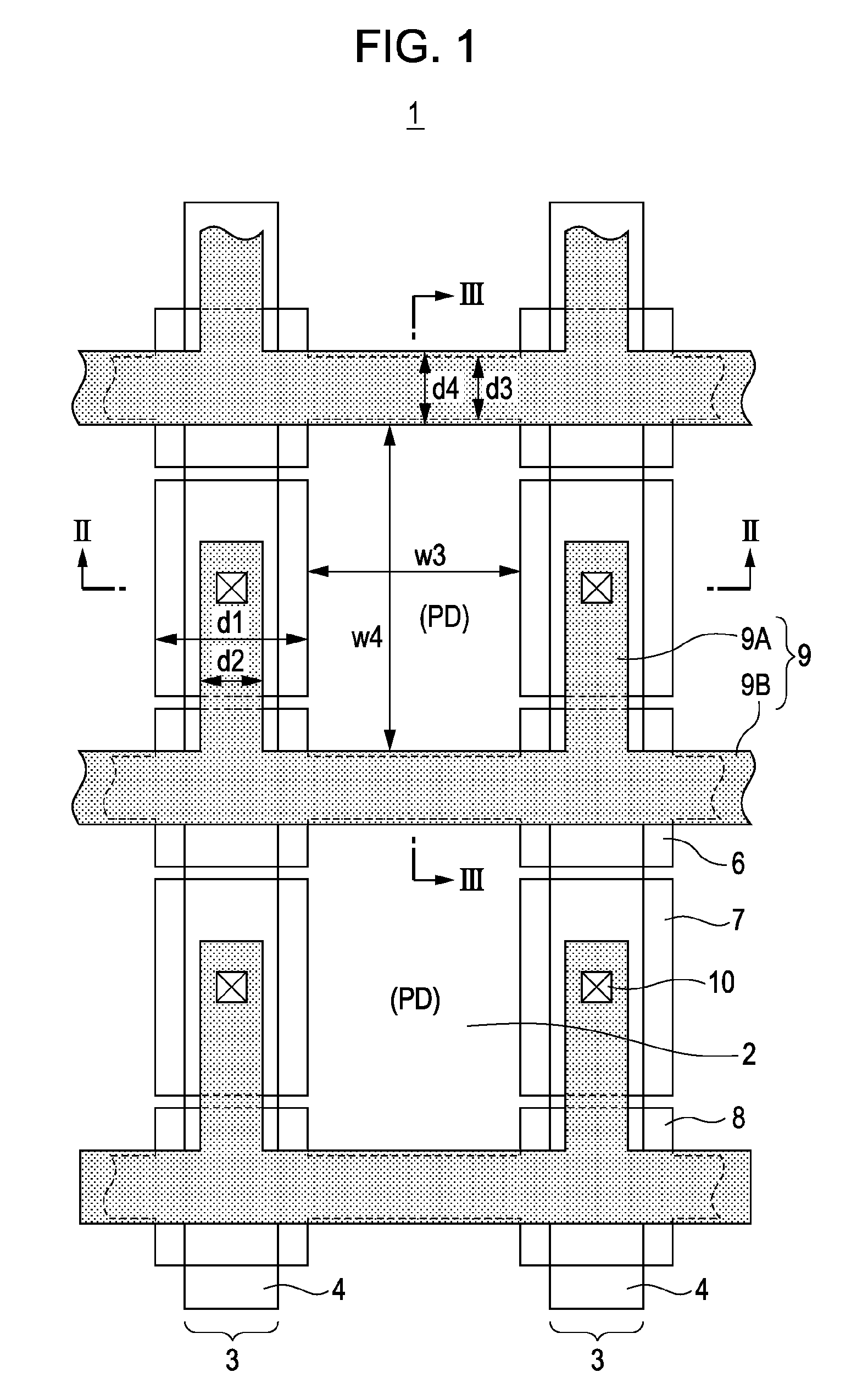
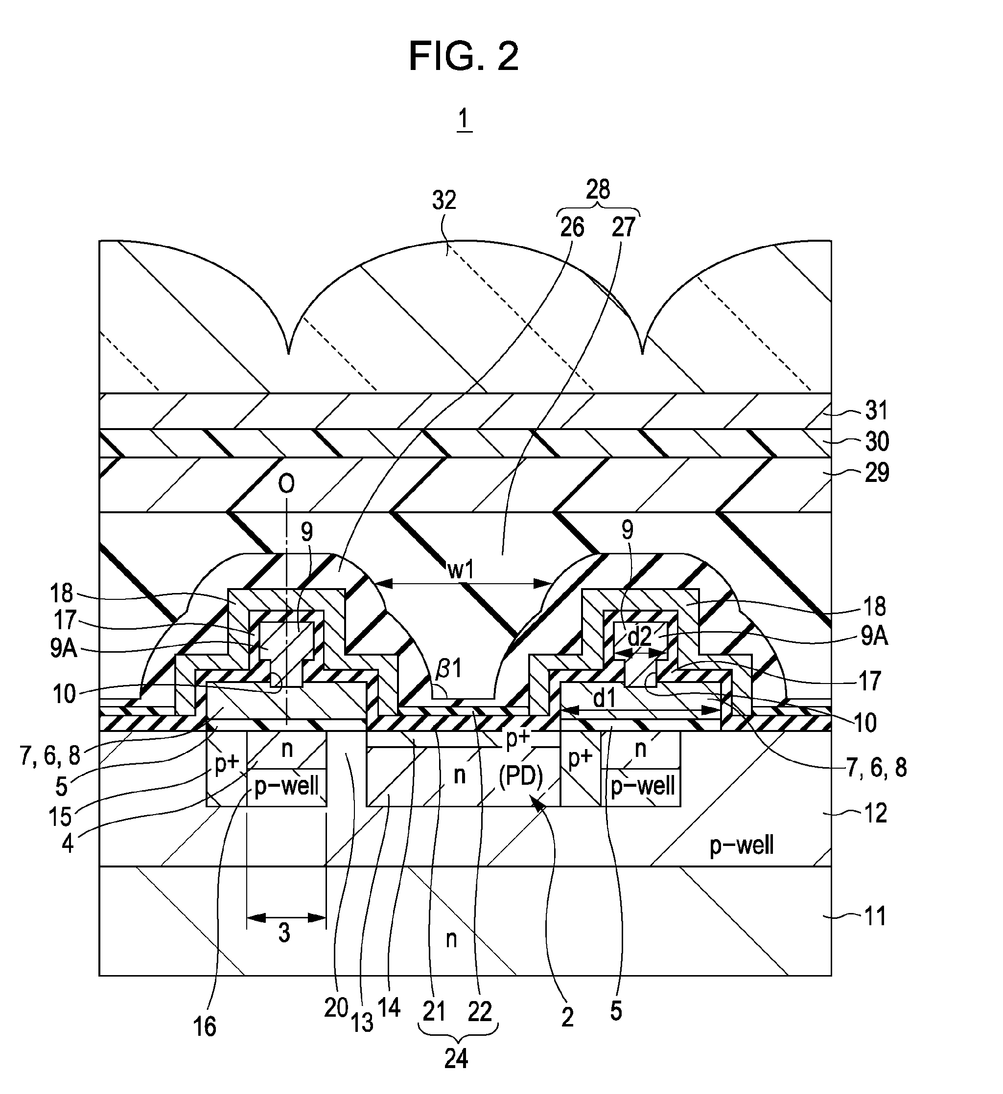
[0095]FIGS. 1 to 3 show an example of a solid-state imaging device according to a first embodiment of the present invention, which is applied to a CCD solid-state imaging device. FIG. 1 is a plan view showing a main portion of an imaging region of a CCD solid-state imaging device, FIG. 2 is a cross-sectional view taken along the line II-II of FIG. 1, and FIG. 3 is a cross-sectional view taken along the line III-III of FIG. 1.

[0096]Referring to FIG. 1, a solid-state imaging device 1 according to the first embodiment has an imaging region including rectangular light-sensing sections 2 which are two-dimensionally arrayed and a vertical transfer register section 3 which has a CCD structure and which is disposed for each column of light-sensing sections 2. Each of the light-sensing sections 2 has a rectangular shape in which w4>w3, where w4 is an opening width in the longitudinal direction, and w3 is an opening width in...

second embodiment

2. Second Embodiment

Example of Structure of Solid-State Imaging Device

[0125]FIG. 10 shows an example of a solid-state imaging device according to a second embodiment of the present invention, which is applied to a CCD solid-state imaging device. FIG. 10 shows a main portion of an imaging region of the solid-state imaging device, in particular, light-sensing sections and waveguides, in which the left portion shows a cross-sectional structure taken in the horizontal direction, and the right portion shows a cross-sectional structure taken in the vertical direction.

[0126]In a solid-state imaging device 41 according to this embodiment, a connecting conductive layer 9 is disposed on each of transfer electrodes 6 to 8 so as to be shifted in the width direction with respect to the axis O of the transfer electrode such that the cross-sectional structure of a waveguide 28 in the horizontal direction of an imaging plane is different from that in the vertical direction. That is, in a vertical t...

third embodiment

3. Third Embodiment

Example of Structure of Solid-State Imaging Device

[0137]FIG. 12 shows an example of a solid-state imaging device according to a third embodiment of the present invention, which is applied to a CCD solid-state imaging device. FIG. 12 shows a main portion of an imaging region of the solid-state imaging device, in particular, light-sensing sections and waveguides, in which the left portion shows a cross-sectional structure taken in the horizontal direction, and the right portion shows a cross-sectional structure taken in the vertical direction.

[0138]In a solid-state imaging device 43 according to this embodiment, the transfer electrodes 6 to 8 and the connecting conductive layers 9 in the vertical transfer register section 3 are formed as in the first embodiment, and waveguides are formed in a three-layered structure including layers having different refractive indices such that the cross-sectional structure of each waveguide in the horizontal direction of the imagin...


PUM


Abstract

A solid-state imaging device includes light-sensing sections serving as pixels, and waveguides each including a core layer and a cladding layer, the waveguides each being disposed at a position corresponding to one of the light-sensing sections. A cross-sectional structure of the waveguide taken in the horizontal direction of an imaging plane is different from a cross-sectional structure of the waveguide taken in the vertical direction of the imaging plane.

Description

BACKGROUND OF THE INVENTION[0001]1. Field of the Invention[0002]The present invention relates to a solid-state imaging device, a method of manufacturing the same, and an electronic apparatus including the solid-state imaging device.[0003]2. Description of the Related Art[0004]Solid-state imaging devices are classified roughly into charge transfer solid-state imaging devices typified by a charge-coupled device (CCD) image sensor and amplification type solid-state imaging devices typified by a complementary metal oxide semiconductor (CMOS) image sensor.[0005]Typically, a CCD solid-state imaging device has an imaging region including a plurality of light-sensing sections, i.e., photodiodes serving as photoelectric conversion elements, which are two-dimensionally arrayed, and a vertical transfer register section which has a CCD structure and which is disposed for each column of photodiodes. The CCD solid-state imaging device further includes a horizontal transfer register section which ...

Claims


Application Information

Patent Timeline
Patent Type & Authority Applications(United States)
IPC IPC(8): H01L31/0232H01L31/18H01L27/14H01L27/148H04N5/335H04N5/369H04N5/372
CPCH01L27/14621H01L27/14627H01L27/14629H01L27/14818H01L27/14812H01L27/146H04N25/00
Inventor WANO, HIROMIKITANO, YOSHIAKI
Owner SONY SEMICON SOLUTIONS CORP
Why Eureka
Try Eureka