Miim diodes

a diode and diode technology, applied in the field of integrated circuits, can solve the problems of low rectification ratio, low breakdown voltage, and insufficient current, and achieve the effect of improving the properties of the diod

Inactive Publication Date: 2010-04-01
SANDISK TECH LLC
View PDF30 Cites 70 Cited by
  • Summary
  • Abstract
  • Description
  • Claims
  • Application Information

AI Technical Summary

Benefits of technology

[0012]Another embodiment is metal-insulator diode that is doped with a material that improves properties of the diode. The diode has a first electrode comprising a first metal and a first region comprising a first insulating material. The first insulating material has a first interface with the first metal, and the first interface has a first conduction band offset. The diode further has a second region comprising a second insulating material. The second insulating material is doped with a doping material. The diode also has a second electrode comprising a second metal. The second insulating material has a second interface with the second metal, and the second interface has a second conduction band offset. The second conduction band offset is greater than the first conduction band offset. In one aspect, the doping material increases the on current of the diode. In one aspect, the doping material in the second insulator material incorporates traps into the second region.

Problems solved by technology

One problem with MIIM diodes is getting a sufficiently high current when under forward bias given the relatively small scale of structures that is desired.
Another problem with MIIM diodes is that the breakdown voltage is typically too low.
A third problem with MIIM diodes is that rectification ratios are too low.
Still another problem is the process complexity of fabricating MIIM diodes.
However, fabricating such thin dielectrics presents challenges.

Method used


Image

  • Miim diodes
  • Miim diodes
  • Miim diodes

Examples


Embodiment Construction

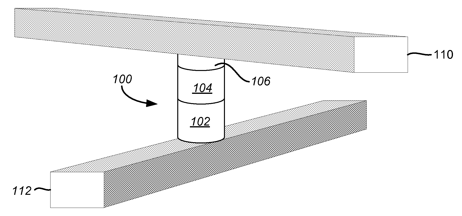
[0029]FIG. 1 depicts an exemplary structure for a non-volatile memory cell that can be used in accordance with embodiments of the present disclosure. A two-terminal memory cell 100 as depicted in FIG. 1 includes a first terminal portion connected to a first conductor 110 and a second terminal portion connected to a second conductor 112. The memory cell includes a steering element 102 in series with a state change element 104 and an anti-fuse 106 to provide non-volatile data storage. The steering element can take the form of any suitable device exhibiting a nonlinear conduction current characteristic such as a simple diode. Various embodiments of MIIM diodes disclosed herein can be used to implement the steering element. The state change element 104 will vary by embodiment and can include numerous types of materials to store data through representative physical states. State change element 104 can include resistance change materials, phase change resistive materials, etc. For example...


PUM

PropertyMeasurementUnit
thickaaaaaaaaaa
thickaaaaaaaaaa
work functionsaaaaaaaaaa

Abstract

A metal-insulator diode is disclosed. In one aspect, the metal-insulator diode comprises a first electrode comprising a first metal, a first region comprising a first insulating material, a second region comprising a second insulating material, and a second electrode comprising a second metal. The first region and the second region reside between the first electrode and the second electrode. The second insulating material is doped with nitrogen. Note that the second insulating material may have an interface with either the first electrode or the second electrode.

Description

CROSS-REFERENCE TO RELATED APPLICATIONS[0001]The following related applications, filed on even date herewith, are cross-referenced and incorporated by reference herein in their entirety:[0002]U.S. patent application Ser. No. ______ (Attorney Docket No. SAND-01343US0), entitled “MIIM DIODES HAVING STACKED STRUCTURE”; and[0003]U.S. patent application Ser. No. ______ (Attorney Docket No. SAND-01370US0), entitled “DAMASCENE PROCESS FOR CARBON MEMORY ELEMENT WITH MIIM DIODE.”BACKGROUND OF THE INVENTION[0004]1. Field of the Invention[0005]Embodiments in accordance with the present disclosure are directed to integrated circuits containing non-volatile memory cell arrays and particularly those arrays incorporating passive element memory cells.[0006]2. Description of the Related Art[0007]Materials having a detectable level of change in state, such as a resistance or phase change, are used to form various types of non-volatile semiconductor based memory devices. For example, simple anti-fuses...

Claims


Application Information

Patent Timeline
Patent Type & Authority Applications(United States)
IPC IPC(8): H01L29/861G11C11/50H01L21/44
CPCH01L27/2418H01L45/00H01L45/145H01L45/149H01L45/06H01L45/144H01L45/04H10B63/22H10N70/00H10N70/231H10N70/20H10N70/8845H10N70/8828H10N70/883
Inventor SEKAR, DEEPAK C.KUMAR, TANMAYRABKIN, PETERCHEN, XIYING
Owner SANDISK TECH LLC
Why Eureka
Try Eureka