Method for forming cobalt nitride cap layers

a cobalt nitride and cap layer technology, applied in the field of semiconductor devices, can solve the problems of affecting the acceptance of this complex process, em and sm have fast become critical challenges, and the electrical defects that can destroy an integrated circuit, so as to improve the effect of electromigration and stress migration

Active Publication Date: 2010-04-01
TOKYO ELECTRON LTD
View PDF14 Cites 16 Cited by
  • Summary
  • Abstract
  • Description
  • Claims
  • Application Information

AI Technical Summary

Benefits of technology

[0007]Embodiments of the invention provide a method for integrating cobalt nitride layers into manufacturing of semiconductor devices to improve electromigration and stress migration in Cu metallization. Embodiments of the invention may be applied to treating a planarized substrate containing Cu paths and dielectric regions prior to selectively forming cobalt nitride cap layers on the Cu paths relative to the dielectric regions. The treating can remove residues and copper oxide from the planarized substrate. In one example, the residues may include organic materials that are used in a chemical mechanical planarization (CMP) process.

Problems solved by technology

The use of copper (Cu) metal in multilayer metallization schemes for manufacturing integrated circuits has created several problems that require solutions.
For example, high mobility of Cu atoms in dielectric materials and Si can result in migration of Cu atoms into those materials, thereby forming electrical defects that can destroy an integrated circuit.
Because electromigration (EM) and stress migration (SM) lifetimes are inversely proportional to current density, EM and SM have fast become critical challenges.
However, maintaining acceptable deposition selectivity on bulk Cu metal, especially for tight pitch Cu wiring, and maintaining good film uniformity, has affected acceptance of this complex process.
Furthermore, wet process steps using acidic solution may be detrimental to the use of CoWP.

Method used


Image

  • Method for forming cobalt nitride cap layers
  • Method for forming cobalt nitride cap layers
  • Method for forming cobalt nitride cap layers

Examples


Embodiment Construction

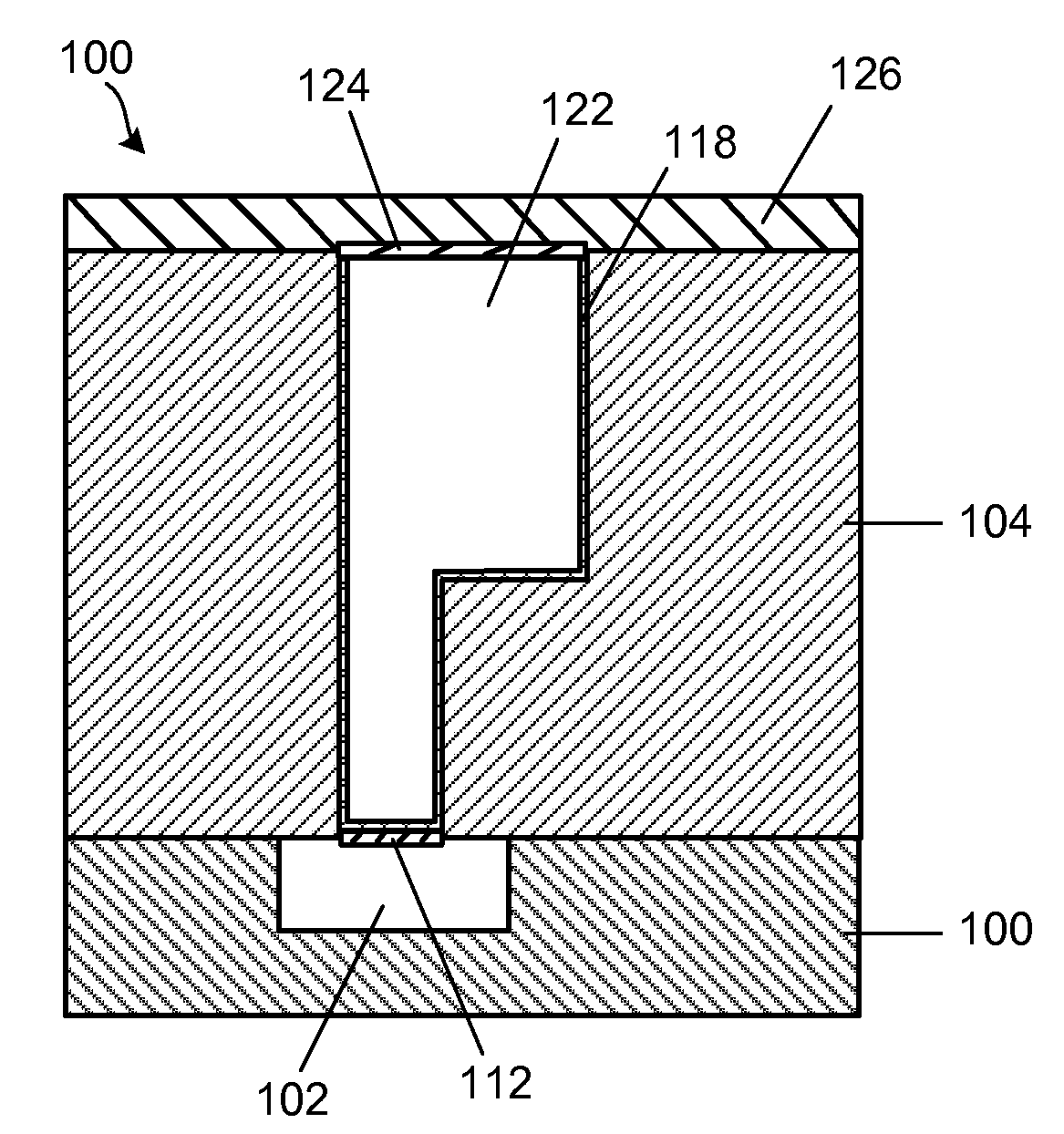
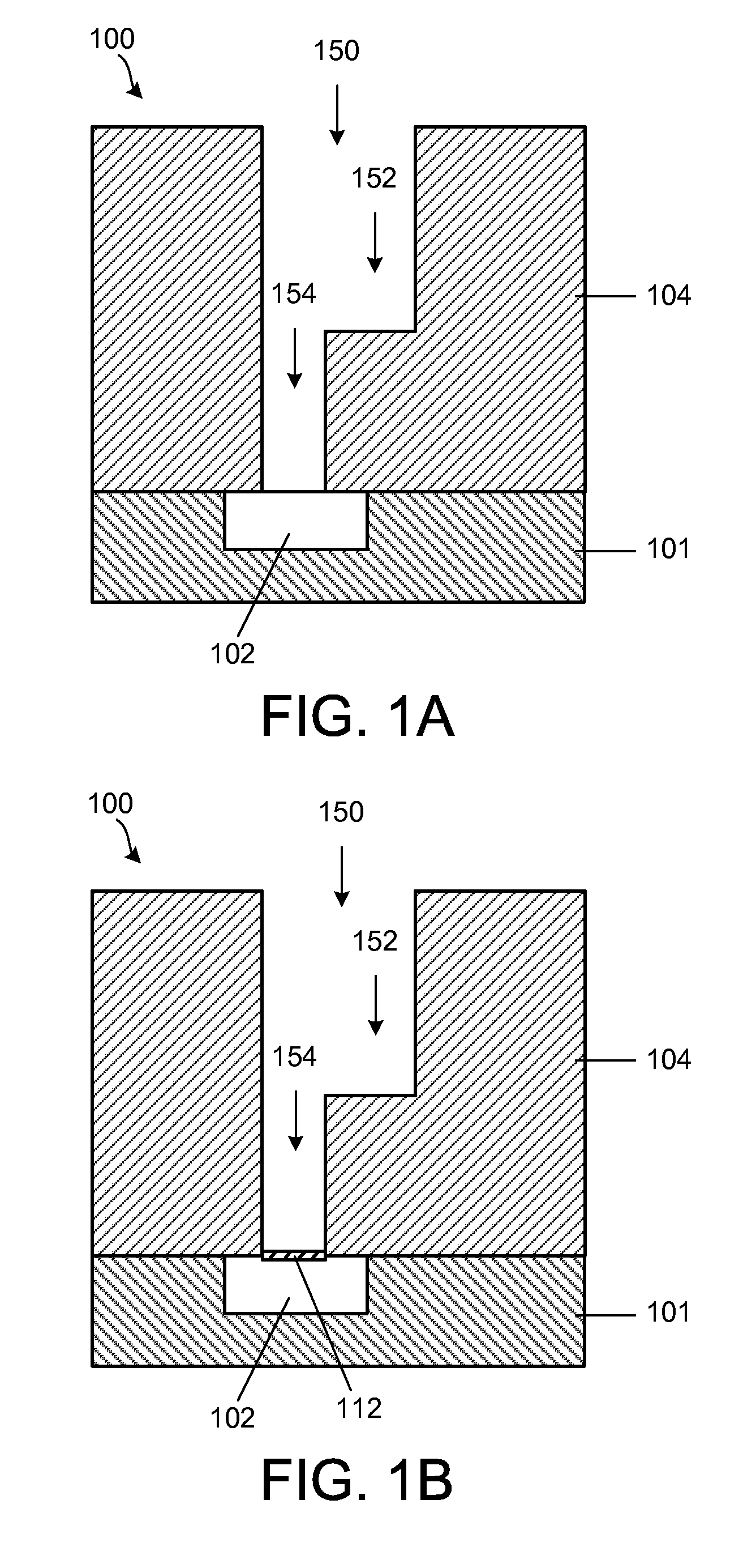
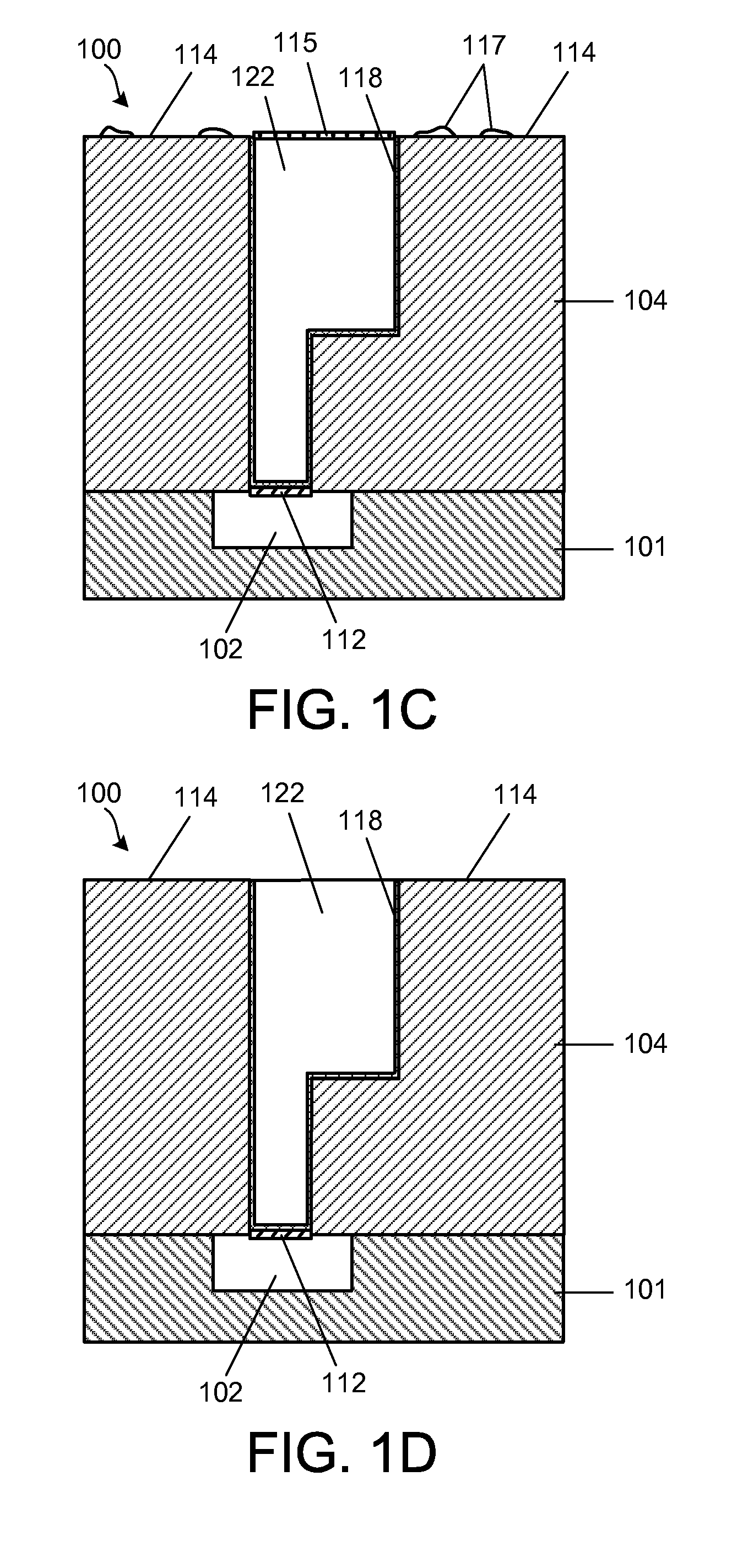
[0014]Embodiments of the invention provide a method for integrating cobalt nitride cap layers into Cu metallization of semiconductor devices to improve electromigration (EM) and stress migration (SM) in the devices and provide good chemical resistance to wet processing steps. The method can provide selectivity for cobalt nitride cap layer deposition on metal surfaces such as Cu paths relative to dielectric surfaces between the Cu paths that results in improved margin for line-to-line breakdown and electrical leakage performance.

[0015]One skilled in the relevant art will recognize that the various embodiments may be practiced without one or more of the specific details, or with other replacement and / or additional methods, materials, or component. In other instances, well-known structures, materials, or operations are not shown or described in detail to avoid obscuring aspects of various embodiments of the invention. Similarly, for purposes of explanation, specific numbers, materials,...


PUM

PropertyMeasurementUnit
widthsaaaaaaaaaa
widthsaaaaaaaaaa
widthsaaaaaaaaaa

Abstract

A method is provided for integrating cobalt nitride cap layers into manufacturing of semiconductor devices to improve electromigration and stress migration in copper (Cu) metal. One embodiment includes providing a patterned substrate containing a recessed feature formed in a low-k material and a first metallization layer at the bottom of the feature, forming a cobalt nitride cap layer on the first metallization layer, depositing a barrier layer in the recessed feature, including on the low-k dielectric material and on the first cobalt metal cap layer, and filling the recessed feature with Cu metal. Another embodiment includes providing a patterned substrate having a substantially planar surface with Cu paths and low-k dielectric regions, and selectively forming a cobalt nitride cap layer on the Cu paths relative to the low-k dielectric regions.

Description

CROSS-REFERENCE TO RELATED APPLICATION[0001]The present invention is related to U.S. patent application Ser. No. ______ (Docket no. TTCA-273), entitled “METHOD FOR FORMING COBALT TUNGSTEN CAP LAYERS”, filed on even date herewith. The entire contents of this application are incorporated herein by reference.FIELD OF THE INVENTION[0002]The present invention relates to semiconductor processing and semiconductor devices, and more particularly, to a method of integrating cobalt (Co) nitride films into the manufacturing of semiconductor devices.BACKGROUND OF THE INVENTION[0003]An integrated circuit contains various semiconductor devices and a plurality of conducting metal paths that provide electrical power to the semiconductor devices and allow these semiconductor devices to share and exchange information. Within the integrated circuit, metal layers are stacked on top of one another using intermetal or interlayer dielectric layers that insulate the metal layers from each other. Normally, ...

Claims


Application Information

Patent Timeline
Patent Type & Authority Applications(United States)
IPC IPC(8): H01L21/768
CPCH01L21/02063H01L21/02074H01L21/76814H01L21/76846H01L21/76849H01L21/76883H01L2924/0002H01L23/53238H01L2924/3011H01L2924/00
Inventor ISHIZAKA, TADAHIROMIZUNO, SHIGERUJOMEN, MIHO
Owner TOKYO ELECTRON LTD
Why Eureka
Try Eureka