

Wiring board and method of fabricating the same
a technology of wiring board and insulator layer, which is applied in the direction of printed circuit aspects, conductive pattern formation, and semiconductor/solid-state device details, etc., can solve the problems of increasing the fabrication cost of the wiring board, affecting the further reduction of the thickness of the wiring board that is fabricated using the build-up, and the inability to suppress the insulator layer satisfactorily. , to achieve the effect of suppressing delamination and improving the reliability of the wiring board
- Summary
- Abstract
- Description
- Claims
- Application Information
AI Technical Summary
Benefits of technology
Problems solved by technology
Method used
Image

Examples
first embodiment
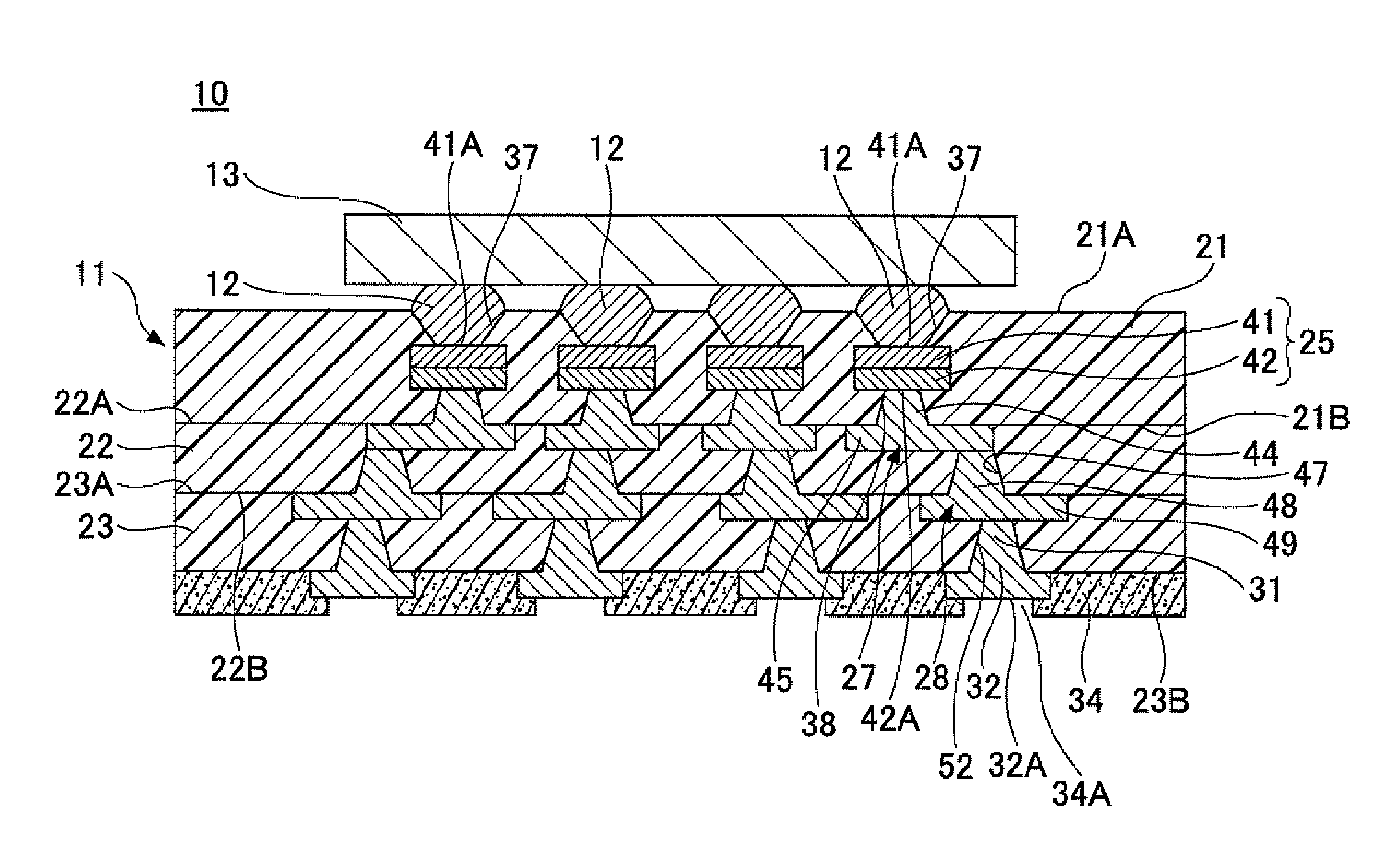
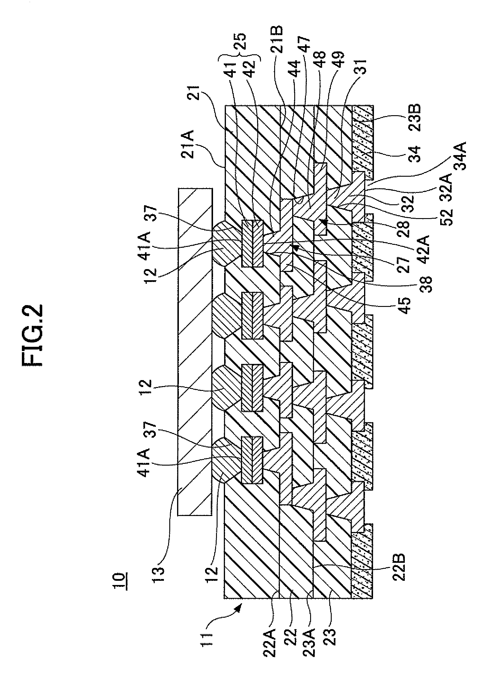
[0037]FIG. 2 is a cross sectional view illustrating a semiconductor device in a first embodiment of the present invention. The semiconductor device according to the present invention is also referred to as a semiconductor package.
[0038]A semiconductor device 10 of this first embodiment includes a wiring board 11 and an electronic component 13. The wiring board 11 includes stacked insulator layers 21, 22 and 23, electrode pads 25, conductor patterns 27 and 28, vias 31, pads 32 for external connection, and a solder resist layer 34.
[0039]The insulator layer 21 is stacked on a surface 22A of the insulator layer 22. The electrode pads 25 and via parts 44 are embedded in the insulator layer 21, and the via part 44 forms a constituent element of the conductor pattern 27. The insulator layer 21 includes openings 37 and 38. The opening 37 is provided in a portion of the insulator layer 21 on the opposite side from a portion of the insulator layer 21 making contact with the surface 22A of the...
second embodiment
[0089]FIG. 18 is a cross sectional view illustrating the semiconductor device in a second embodiment of the present invention. In FIG. 18, those parts that are the same as those corresponding parts of the semiconductor device 10 of the first embodiment illustrated in FIG. 2 are designated by the same reference numerals.
[0090]As illustrated in FIG. 18, a semiconductor device 70 in this second embodiment is provided with a wiring board 71, in place of the wiring board 11 provided in the semiconductor device 10 of the first embodiment. Otherwise, the structure of the semiconductor device 70 is basically the same as that of the semiconductor device 10.
[0091]The wiring board 71 is provided with electrode pads 73, in place of the electrode pads 25 provided in the wiring board 11. Otherwise, the structure of the wiring board 71 is basically the same as that of the wiring board 11.
[0092]The electrode pad 73 includes, in addition to the structure of the electrode pad 25, a third metal layer ...
third embodiment
[0149]FIG. 40 is a cross sectional view illustrating the semiconductor device in a third embodiment of the present invention. In FIG. 40, those parts that are the same as those corresponding parts of the semiconductor device 70 of the second embodiment illustrated in FIG. 18 are designated by the same reference numerals.
[0150]As illustrated in FIG. 40, a semiconductor device 85 in this third embodiment is provided with a wiring board 86 in place of the wiring board 71 of the semiconductor device 70 of the second embodiment. Otherwise, the structure of the semiconductor device 85 is basically the same as that of the semiconductor device 70.
[0151]The wiring board 86 has electrode pads 88 in place of the electrode pads 73 of the wiring board 71. Otherwise, the structure of the wiring board 86 is basically the same as that of the wiring board 71.
[0152]In the electrode pad 88, the outer peripheral side surfaces of the (second) metal layer 42 are disposed on the inner side compared to the...
PUM
| Property | Measurement | Unit |
|---|---|---|
| width | aaaaa | aaaaa |
| width | aaaaa | aaaaa |
| diameter | aaaaa | aaaaa |
Abstract
Description
Claims
Application Information