Solid-state imaging element, driving method therefor, and camera system

a technology of solid-state imaging and driving method, which is applied in the direction of color television details, television system, radioation controlled devices, etc., can solve problems such as circuit size increase, and achieve the effect of preventing an increase in circuit siz

Active Publication Date: 2010-04-08
SONY SEMICON SOLUTIONS CORP
View PDF7 Cites 25 Cited by
  • Summary
  • Abstract
  • Description
  • Claims
  • Application Information

AI Technical Summary

Benefits of technology

[0037]According to an embodiment of the present invention, therefore, blooming can be prevented from occurring and an unnecessary row of pixel data can be prevented from being output to the outside while preventing an increase in the circuit size.

Problems solved by technology

No. 2006-310932, however, has the disadvantage of increasing the number of necessary circuits, leading to an increase in circuit size.

Method used


Image

  • Solid-state imaging element, driving method therefor, and camera system
  • Solid-state imaging element, driving method therefor, and camera system
  • Solid-state imaging element, driving method therefor, and camera system

Examples


first embodiment

[0054]FIG. 3 is a diagram showing an example configuration of a CMOS image sensor (solid-state imaging element) 100 according to a first embodiment of the present invention.

[0055]The CMOS image sensor 100 according to the first embodiment includes a pixel array unit 110, a row read control circuit 120, a row reset control circuit 130, a parallel signal processing circuit 140, an output control circuit 150, and a timing control circuit 160.

[0056]The row read control circuit 120, the row reset control circuit 130, and the timing control circuit 160 may constitute a pixel drive control unit.

[0057]The pixel array unit 110 has a two-dimensional array of pixel circuits which are arranged in a matrix.

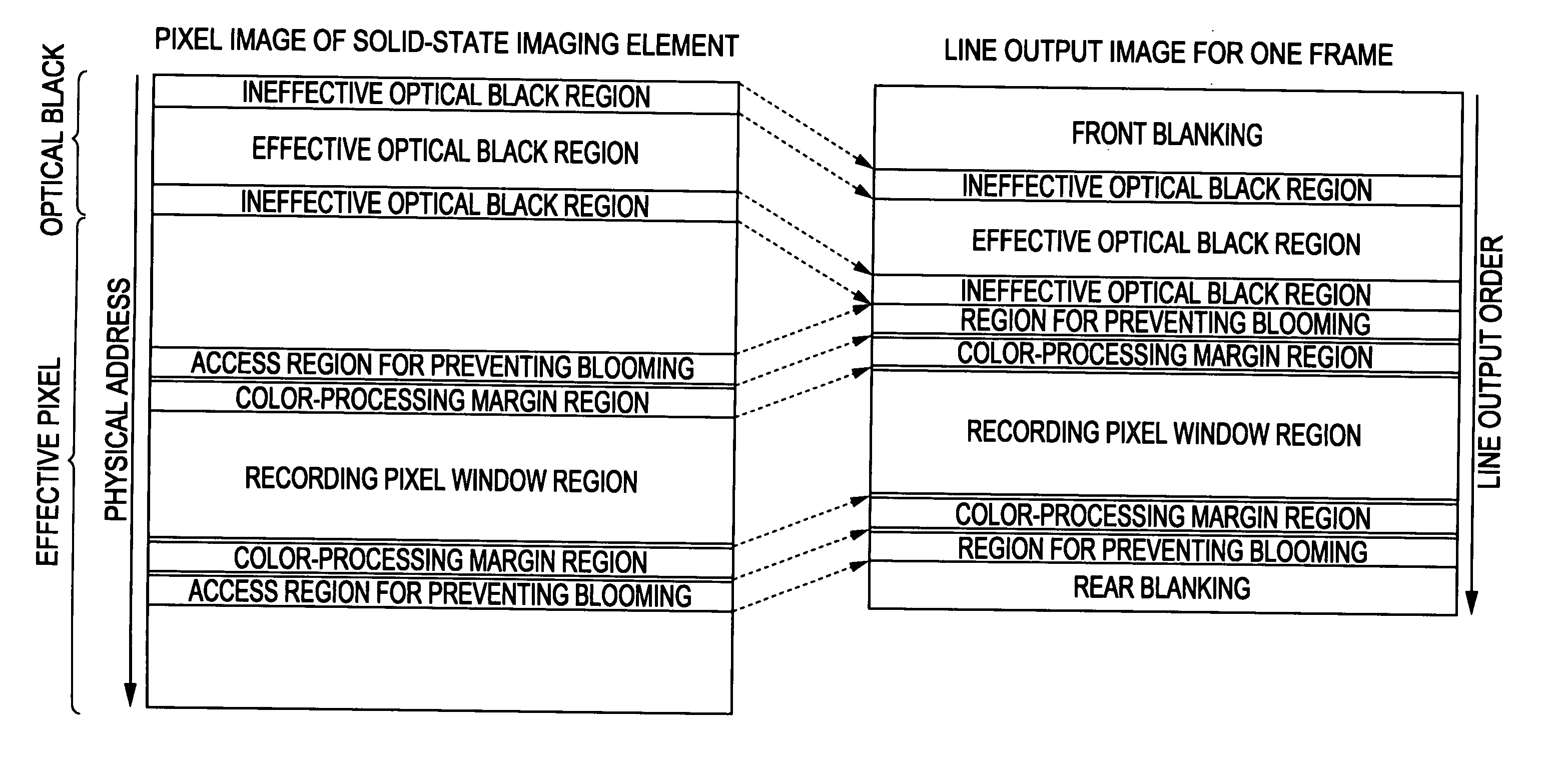
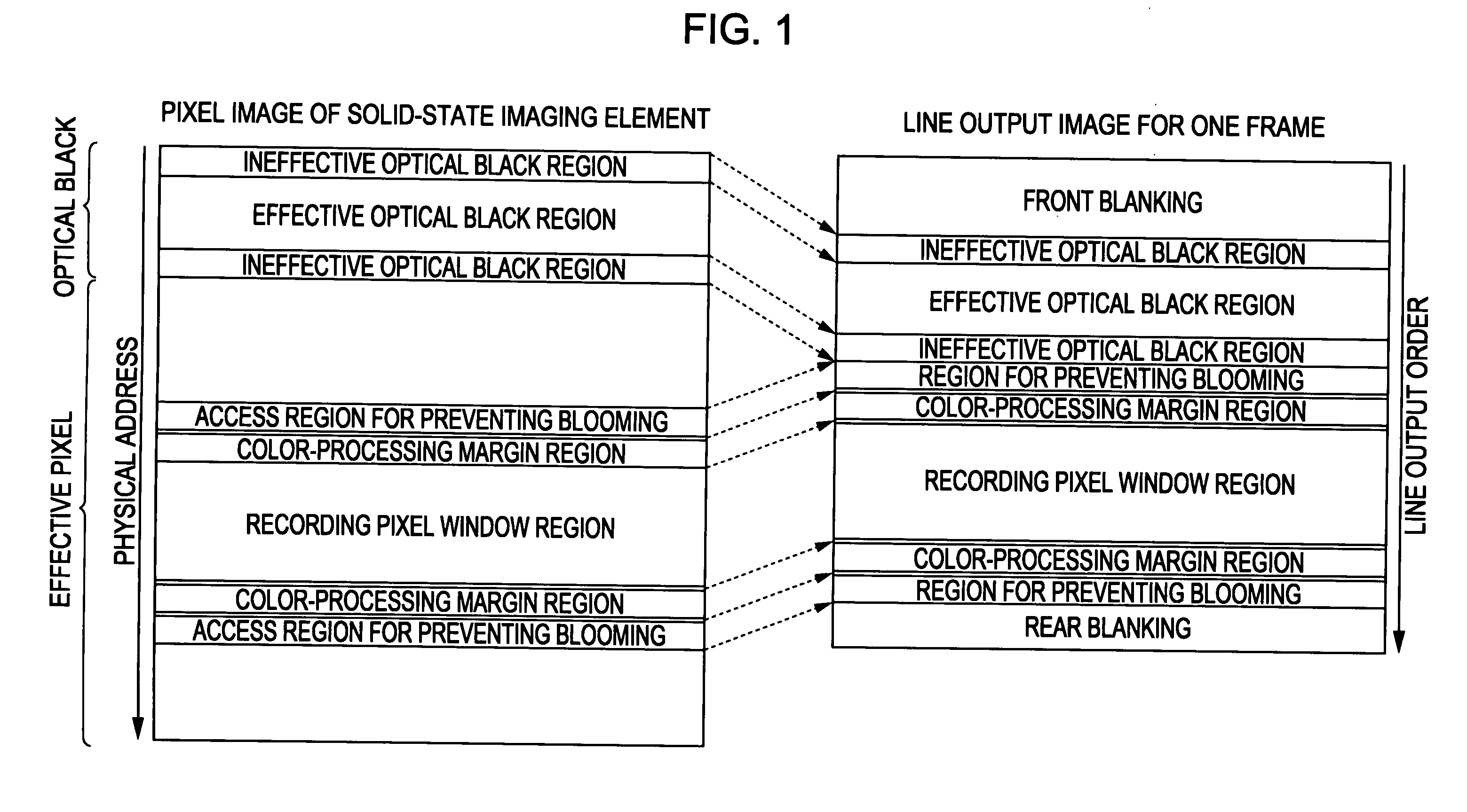
[0058]The pixel array unit 110 includes an effective pixel region 110A, and a light-blocking pixel region (optical black region) 110B defined along the periphery of the effective pixel region 110A.

[0059]The effective pixel region 110A may be a region where signals obtained using photoelectric ...

second embodiment

[0194]FIG. 11 is a diagram showing an example configuration of a CMOS image sensor (solid-state imaging element) 100A according to a second embodiment of the present invention.

[0195]The CMOS image sensor 100A according to the second embodiment is different from the CMOS image sensor 100 according to the first embodiment in that a row access shift register 170 is arranged in place of the row read control circuit 120 and row reset control circuit 130 shown in FIG. 3.

[0196]Also in the second embodiment, the timing control circuit 160 controls the row access shift register 170 using a method similar to that in the first embodiment, thereby achieving the same or similar advantages.

[0197]According to the present embodiment, therefore, the following advantages can be achieved.

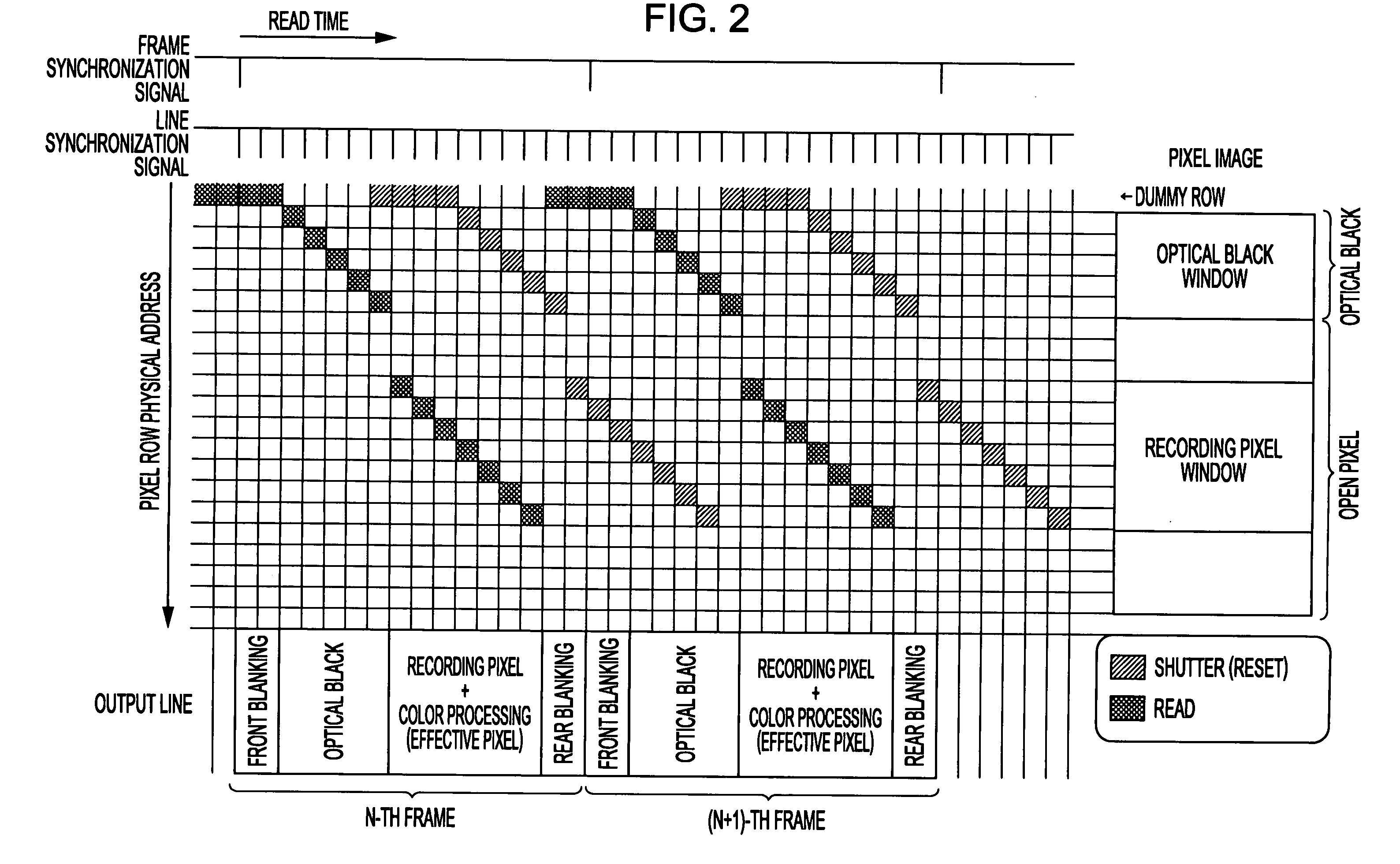
[0198](1) Read access or shutter (reset) access to a row adjacent to a window region can be carried out to prevent blooming.

[0199]The access to an adjacent row is performed for a period during which blanking data is o...

third embodiment

[0216]FIG. 14 is a diagram showing an example configuration of a solid-state imaging element (CMOS image sensor) 200 having a column-parallel ADC structure according to a third embodiment of the present invention.

[0217]As shown in FIG. 14, the solid-state imaging element 200 includes a pixel array unit 210 which may serve as an imaging unit, a vertical scanning circuit 220, a horizontal transfer scanning circuit 230, and a timing control circuit 240. The vertical scanning circuit 220, the horizontal transfer scanning circuit 230, and the timing control circuit 240 may serve as a pixel driving unit (pixel array control circuit).

[0218]The solid-state imaging element 200 further includes an ADC group 250, a digital-analog converter (DAC) 260, an amplifying circuit (signal amplifier (S / A)) 270, and a signal processing circuit 280.

[0219]In the above configuration, the vertical scanning circuit 220 has functions corresponding to the functions of the row read control circuit 120 and the ro...


PUM


Abstract

A solid-state imaging element includes a pixel array unit having pixels arranged in a matrix, each pixel including a photoelectric conversion element, and a pixel drive control unit capable of controlling driving of the pixel array unit so as to perform a read or reset access operation of the pixel array unit in accordance with specified address information. The pixel drive control unit is capable of setting a desired region in the pixel array unit as a window region to be accessed. The pixel drive control unit includes a function for performing, concurrently with access to the window region and output processing, read or reset access on at least one adjacent outer row that is adjacent to the window region.

Description

BACKGROUND OF THE INVENTION[0001]1. Field of the Invention[0002]The present invention relates to a solid-state imaging element such as a complementary metal oxide semiconductor device (CMOS) image sensor, a driving method therefor, and a camera system.[0003]2. Description of the Related Art[0004]In recent years, CMOS image sensors have attracted attention as solid-state imaging elements (image sensors) replacing charge coupled device (CCD) image sensors.[0005]CMOS image sensors have overcome the following problems:[0006]The manufacture of CCD pixels involves special processes, and a plurality of power supply voltages are used to operate them. In addition, it is necessary to operate a plurality of peripheral integrated circuits (ICs) in combination.[0007]Such CCD technology increases system complexity. These various problems have been overcome by the CMOS image sensors.[0008]X-Y addressing solid-state imaging elements such as the CMOS image sensors are configured to perform pixel sel...

Claims


Application Information

Patent Timeline
Patent Type & Authority Applications(United States)
IPC IPC(8): H04N5/335H01L27/146H04N5/345H04N5/359H04N5/369H04N5/374
CPCH04N5/378H04N5/3454H04N25/443H04N25/75H04N25/44H04N25/76
Inventor HORIGUCHI, HIROSHI
Owner SONY SEMICON SOLUTIONS CORP
Why Eureka
Try Eureka