Module having a stacked passive element and method of forming the same

a passive element and module technology, applied in the direction of basic electric elements, transformers/reacts mounting/support/suspension, transformers/inductance details, etc., can solve the problems of inability to meet the requirements of the design and manufacturing approach, and the device also provides inadequate heat dissipation capability or reduce the size of the power modul

Active Publication Date: 2010-04-08
INTEL CORP
View PDF100 Cites 57 Cited by
  • Summary
  • Abstract
  • Description
  • Claims
  • Application Information

AI Technical Summary

Benefits of technology

[0009]These and other problems are generally solved or circumvented, and technical advantages are generally achieved, by advantageous embodiments of the present invention, which include a module having a discrete passive element and a semiconductor device, and method of forming the same. In one embodiment, the module (e.g., a power module) includes a patterned leadframe, a discrete passive element (e.g., a discrete magnetic device) mounted on an upper surface of the leadframe, and a thermally conductive, electrically insulating material formed on an upper surface of the discrete passive element. The module also includes a semiconductor device bonded to an upper surface of the thermally conductive, electrically insulating material.

Problems solved by technology

An area that has been more challenging is to produce a power module that includes larger passive elements, such as inductors, that are difficult to include in an integrated circuit, with an active element that may include control circuit elements and passive elements such as resistors on the same die.
A characteristic that affects broad market acceptance of a power module is its physical size, which introduces thermal design challenges.
The dissipation of heat from these sources is performed in a challenging external thermal environment without compromising a power rating of the power module.
Each of the magnetic devices disclosed in the aforementioned references suffers from a current limitation therefor, which is an impractical design and manufacturing approach for a mass market.
The aforementioned magnetic devices also provide inadequate heat dissipation capability or reduction in the size thereof.
The aforementioned magnetic device also provides inadequate heat dissipation capability or reduction in the size of a power module.
Thus, the designs for power modules of the past are inadequate to produce a sufficiently miniaturized, high-density device with a substantial power rating.
The design of power modules is inadequately served by these aforementioned limitations.

Method used


Image

  • Module having a stacked passive element and method of forming the same
  • Module having a stacked passive element and method of forming the same
  • Module having a stacked passive element and method of forming the same

Examples


Embodiment Construction

[0017]The making and using of the presently preferred embodiments are discussed in detail below. It should be appreciated, however, that the present invention provides many applicable inventive concepts that can be embodied in a wide variety of specific contexts. The specific embodiments discussed are merely illustrative of specific ways to make and use the invention, and do not limit the scope of the invention.

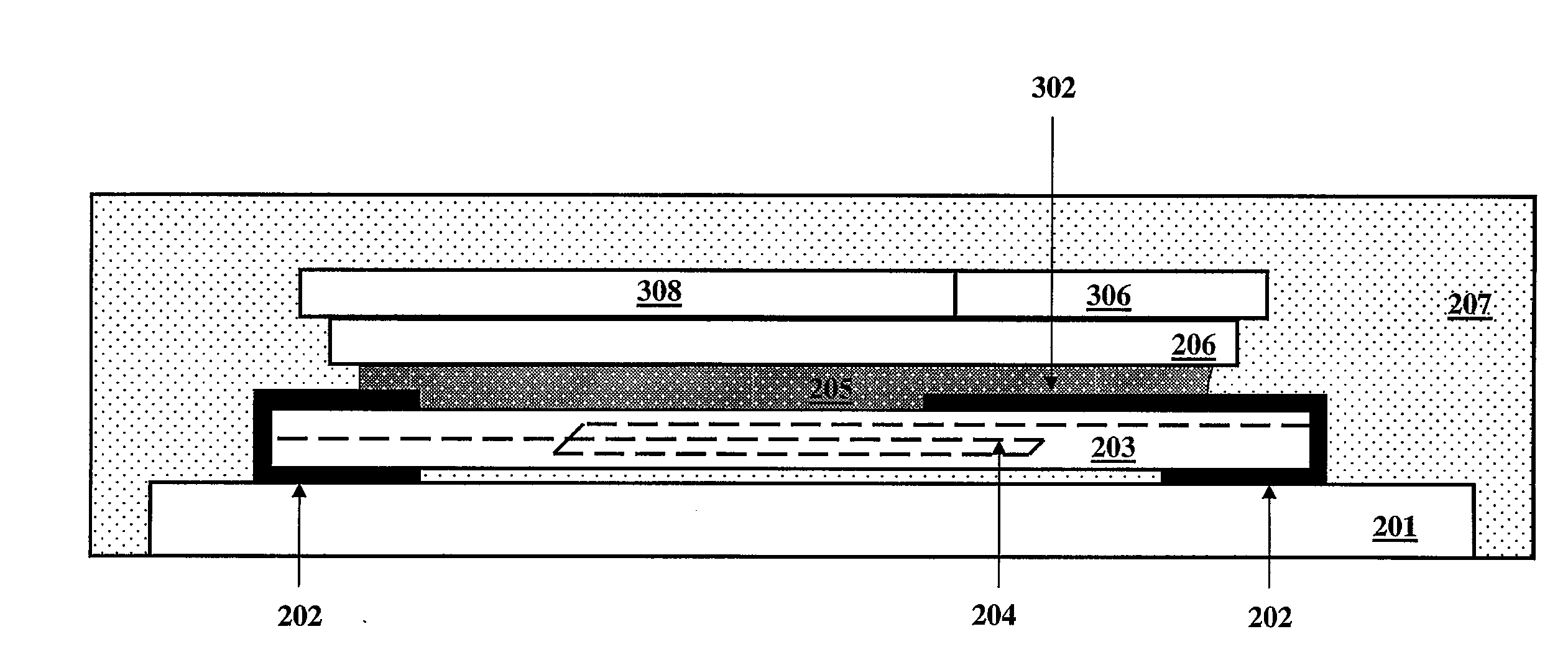
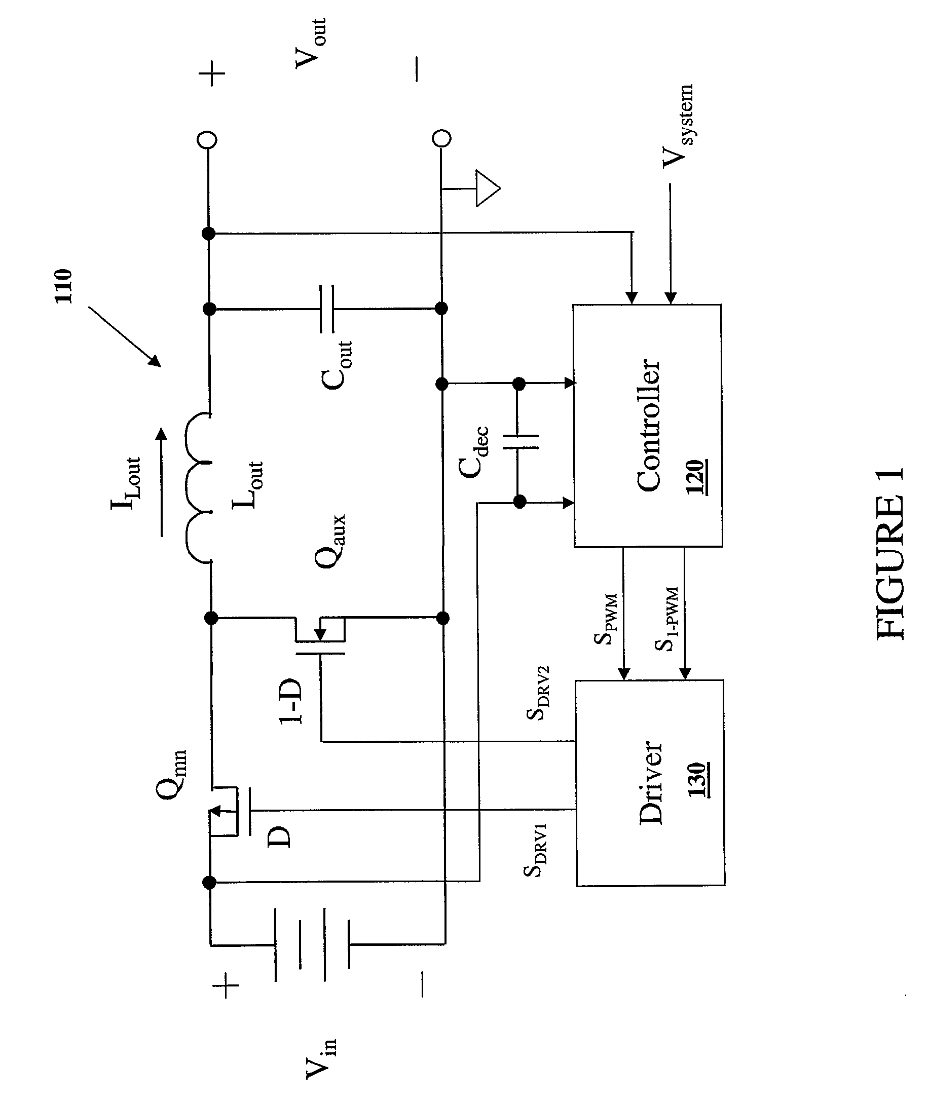
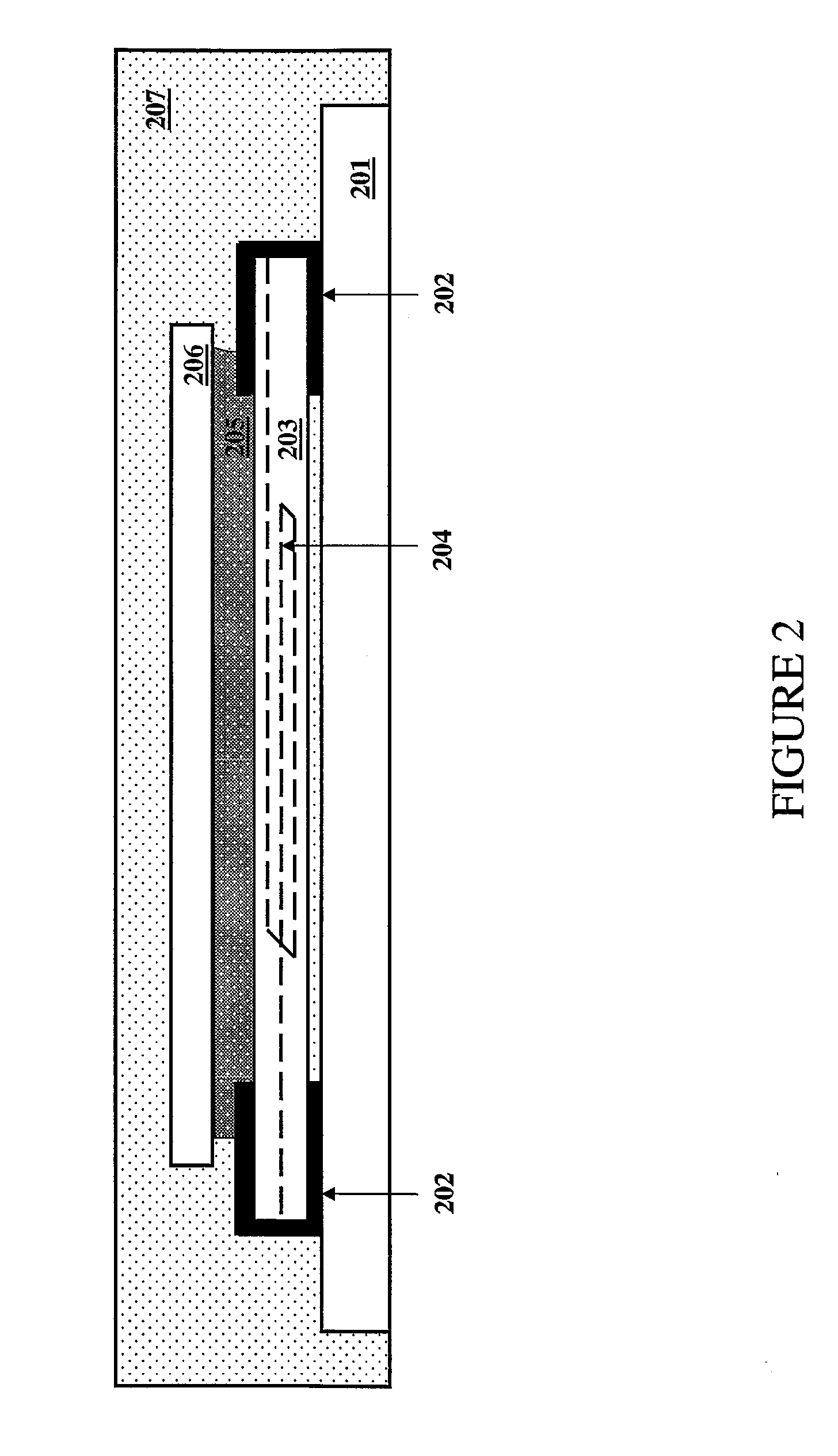
[0018]The present invention will be described with respect to preferred embodiments in a specific context, namely, a power module (e.g., an electronic device) including a discrete or separate passive element and a semiconductor device, and a method of manufacture therefor. While the principles of the present invention will be described in the environment of a power module, any application that may benefit from a semiconductor device mounted on a discrete passive element as described herein is well within the broad scope of the present invention.

[0019]As will become more appar...


PUM


Abstract

A module having a discrete passive element and a semiconductor device, and method of forming the same. In one embodiment, the module includes a patterned leadframe, a discrete passive element mounted on an upper surface of the leadframe, and a thermally conductive, electrically insulating material formed on an upper surface of the discrete passive element. The module also includes a semiconductor device bonded to an upper surface of the thermally conductive, electrically insulating material.

Description

TECHNICAL FIELD[0001]The present invention is directed, in general, to electronic devices and, in particular, to a stacked passive element in a module, and related methods of forming the same.BACKGROUND[0002]Magnetic devices such as inductors are often used in circuit design for electronic devices (e.g., power modules) in which energy is stored in a magnetic field surrounding an electrically conductive element such as a coil of copper wire. To produce an inductor that can store a useful amount of energy for a given size and a given current level, a number of electrically conductive turns or wires are formed around a magnetic structure or core such as a layer of magnetic material. The magnetic field is enhanced by the permeability of the magnetic material and by the presence of the multiple conductive turns. As the size of electronic devices has been reduced by using integrated circuits and printed wiring boards with surface-mount assembly techniques, the size of inductors has not, t...

Claims


Application Information

Patent Timeline
Patent Type & Authority Applications(United States)
IPC IPC(8): H01L21/00
CPCH01L23/3107H01L23/49541H01L2924/1306H01L2924/01015H01L2224/45147H01L2224/45144H01L2924/014H01L2924/01074H01L2924/01033H01L2924/01006H01L24/48H01L2924/19103H01L2924/19041H01L2924/01327H01L2924/01082H01L23/49589H01L23/645H01L24/49H01L25/16H01L2224/48247H01L2224/48465H01L2224/49113H01L2924/01013H01L2924/01028H01L2924/01029H01L2924/01047H01L2924/0105H01L2924/01079H01L2924/00H01L24/45H01L2224/05554H01L2924/00014H01L2924/14H01L2924/181H01L2924/00015H01L2224/05599H01L2924/00012
Inventor LOTFI, ASHRAF W.LOPATA, DOUGLAS DEANWELD, JOHN DAVIDWILKOWSKI, MATHEW A.
Owner INTEL CORP
Why Eureka
Try Eureka