Photoelectrochemical etching for chip shaping of light emitting diodes

a technology of light-emitting diodes and photoelectrochemical etching, which is applied in the direction of electrical equipment, semiconductor devices, solid-state devices, etc., can solve the problems of most of the light reflecting back into the material, the loss of material, and the limitation of external quantum efficiency

Inactive Publication Date: 2010-04-15
RGT UNIV OF CALIFORNIA
View PDF52 Cites 28 Cited by
  • Summary
  • Abstract
  • Description
  • Claims
  • Application Information

AI Technical Summary

Benefits of technology

[0027]As a result, the present invention further discloses an LED, comprising III-Nitride semiconductor material comprising an active region for generating and emitting light; one or more etched surfaces of the III-Nitride material that have a surface smoothness; and an inclination of the surfaces at one or more sloped angles relative to a light emitting surface of the active region, wherein the inclination and the surface smoothness enhance extraction of the light emitted into guided modes trapped in the III-Nitride semiconductor material.

Problems solved by technology

In LEDs, especially in GaN (gallium nitride) and GaP (gallium phosphide) based devices, external quantum efficiency is limited by light emitted into guided modes trapped in the material.
Typically, when wafers are diced, the resulting sidewalls are smooth and vertical, resulting in most of the light reflecting back into the material, where it is eventually lost, with only a small percentage of light being extracted into air.
However, in III-V semiconductor based devices, etching processes are limited because there is no simple wet etch available.
Moreover, both wet and dry etching gives very little control over the angle of the resulting etched sidewalls, providing few options for chip shapes.

Method used


Image

  • Photoelectrochemical etching for chip shaping of light emitting diodes
  • Photoelectrochemical etching for chip shaping of light emitting diodes
  • Photoelectrochemical etching for chip shaping of light emitting diodes

Examples


Embodiment Construction

[0037]In the following description of the preferred embodiment, reference is made to the accompanying drawings which form a part hereof, and in which is shown by way of illustration a specific embodiment in which the invention may be practiced. It is to be understood that other embodiments may be utilized and structural changes may be made without departing from the scope of the present invention.

[0038]Overview

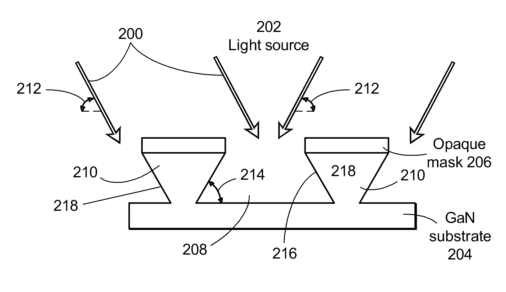
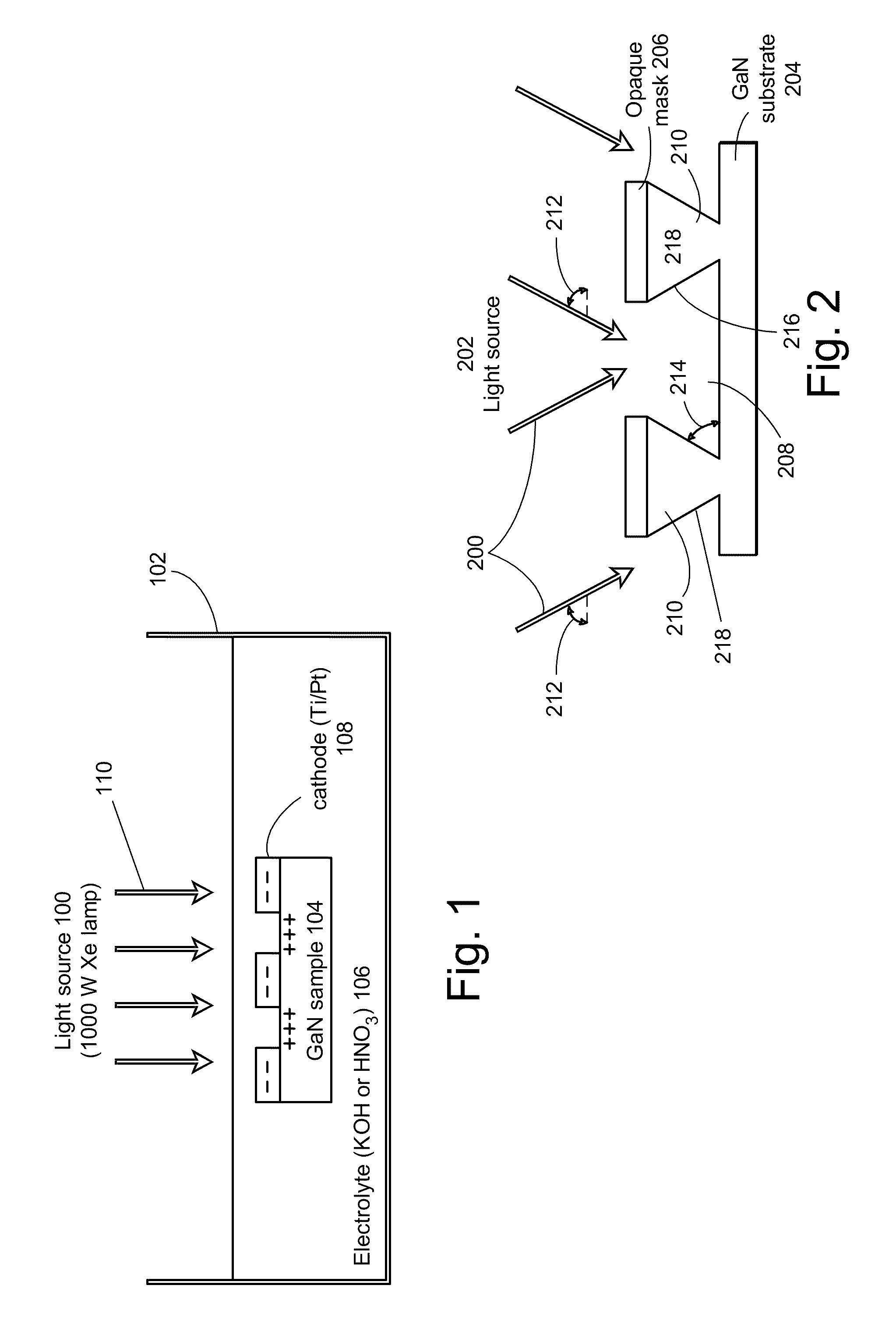
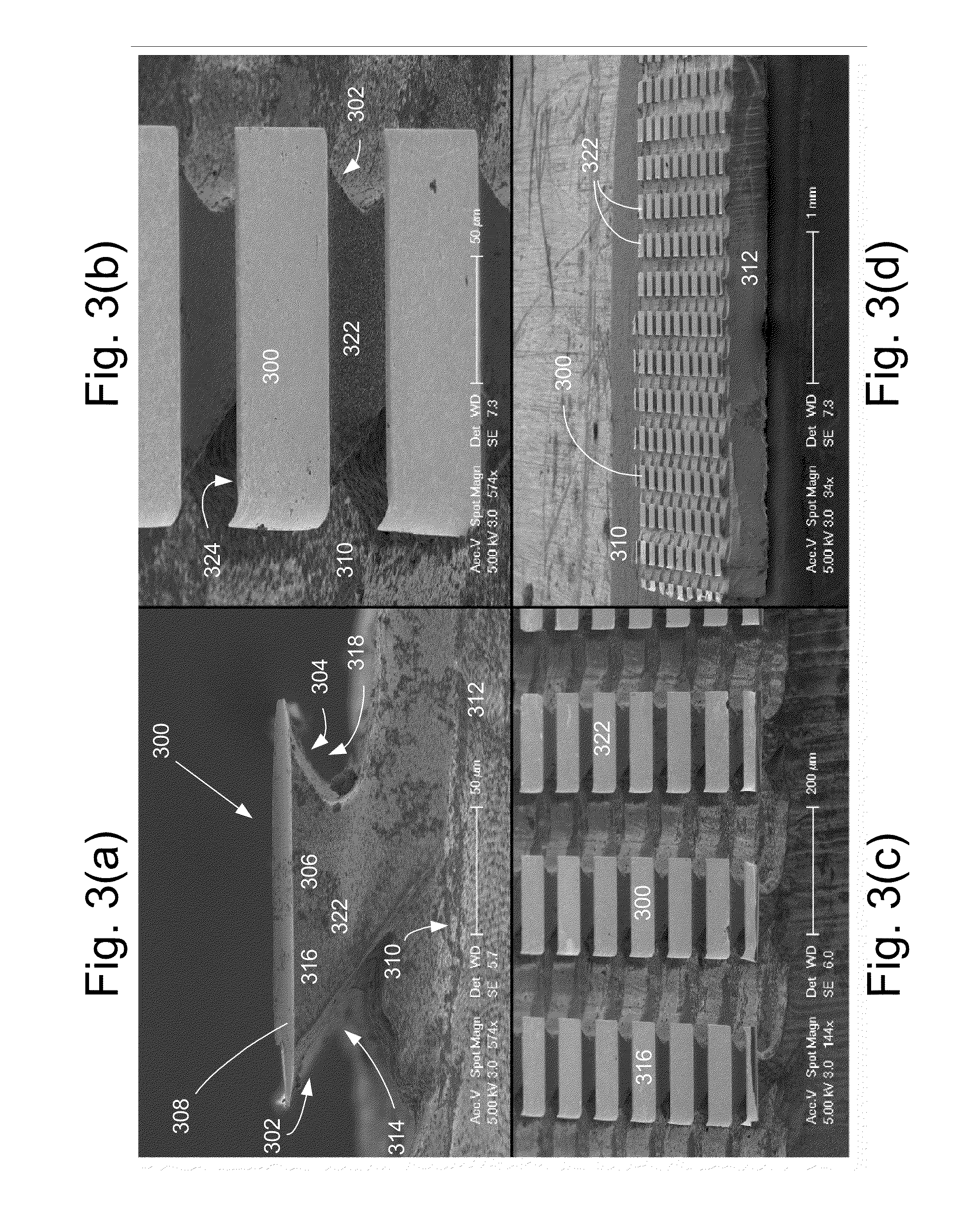
[0039]The present invention describes the use of PEC etching for chip shaping of III-V semiconductor based devices, such as GaN-based and GaAs-based LEDs. Using the technique of the present invention, the material in between LEDs when they are grown on III-V substrates can be directly etched, and by varying the angle of incident light, the angle of the resulting sidewalls can be controlled, resulting in sloped sidewalls, which will scatter guided modes out of the material rather than reflecting them back. Using PEC etching, non-rectilinear chip shapes can be obtained by contro...


PUM

PropertyMeasurementUnit
red wavelengthsaaaaaaaaaa
light extraction efficiencyaaaaaaaaaa
angleaaaaaaaaaa

Abstract

A photoelectrochemical (PEC) etch is performed for chip shaping of a device comprised of a III-V semiconductor material, in order to extract light emitted into guided modes trapped in the III-V semiconductor material. The chip shaping involves varying an angle of incident light during the PEC etch to control an angle of the resulting sidewalls of the III-V semiconductor material. The sidewalls may be sloped as well as vertical, in order to scatter the guided modes out of the III-V semiconductor material rather than reflecting the guided modes back into the III-V semiconductor material. In addition to shaping the chip in order to extract light emitted into guided modes, the chip may be shaped to act as a lens, to focus its output light, or to direct its output light in a particular way.

Description

CROSS REFERENCE TO RELATED APPLICATION[0001]This application claims the benefit under 35 U.S.C. Section 119(e) of co-pending and commonly-assigned U.S. Provisional Application Ser. No. 61 / 104,015 filed on Oct. 9, 2008, by Adele Tamboli, Evelyn L. Hu and James S. Speck, entitled “PHOTOELECTROCHEMICAL ETCHING FOR CHIP SHAPING OF LIGHT EMITTING DIODES,” attorney's docket number 30794.289-US-P1 (2009-157), which application is incorporated by reference herein.[0002]This application is related to the following co-pending and commonly-assigned U.S. patent applications:[0003]U.S. Utility application Ser. No. 10 / 581,940, filed on Jun. 7, 2006, by Tetsuo Fujii, Yan Gao, Evelyn. L. Hu, and Shuji Nakamura, entitled “HIGHLY EFFICIENT GALLIUM NITRIDE BASED LIGHT EMITTING DIODES VIA SURFACE ROUGHENING,” attorney's docket number 30794.108-US-WO (2004-063), which application claims the benefit under 35 U.S.C Section 365(c) of PCT Application Serial No. US2003 / 039211, filed on Dec. 9, 2003, by Tetsu...

Claims


Application Information

Patent Timeline
Patent Type & Authority Applications(United States)
IPC IPC(8): H01L33/00H01L21/78H01L21/306
CPCH01L33/0062H01L33/20H01L33/0079H01L33/0093H01L33/22
Inventor TAMBOLI, ADELEHU, EVELYN L.SPECK, JAMES S.
Owner RGT UNIV OF CALIFORNIA
Why Eureka
Try Eureka