Method for manufacturing a metal and dielectric nanostructures electrode for colored filtering in an OLED and method for manufacturing an OLED

a technology of dielectric nanostructures and dielectric nanostructures, which is applied in the direction of semiconductor/solid-state device manufacturing, electric devices, solid-state devices, etc., can solve the problems of short circuit between electrodes, unusable oled stack, and poor resistance of the emitted molecules of these layers to all the treatments

Inactive Publication Date: 2011-06-23
COMMISSARIAT A LENERGIE ATOMIQUE ET AUX ENERGIES ALTERNATIVES
View PDF6 Cites 36 Cited by
  • Summary
  • Abstract
  • Description
  • Claims
  • Application Information

AI Technical Summary

Benefits of technology

[0091]In particular, the method according to the invention does not include any chemical mechanical polishing step and the method according to the invention consequently avoids all the drawbacks related to this operation. Notably, with the method according to the invention nanostructurations may easily be made with different pattern densities without it being necessary to use fictitious patterns, required during this chemical mechanical polishing. By suppressing, by means of the method according to the invention, these fictitious patterns, the emission surface is thereby increased.
[0092]Accordingly, with the method according to the invention, pixels may easily be made side by side with different colored filterings.
[0093]The method according to the invention globally enhances the extraction of light from the OLED and makes it possible to electrically address each pixel individually.
[0095]The method according to the invention is simple, reliable, easy to apply and with it, it is possible to easily prepare in a controlled, reproducible way, surfaces for which nanostructuration is perfectly, accurately monitored, controlled.
[0096]The shape of the patterns composing the extraction lattices of the diode is generally perfectly controlled, and enhanced but also specifically modulated extraction may be obtained.

Problems solved by technology

However, a poorly controlled structuration may cause both electrodes to be short-circuited, making the OLED stack unusable.
Experiment shows that the emitting molecules of these layers poorly withstand all the treatments occurring>after globally making the diodes.
Further, both in the case of the nano-imprinting technique and in the case of the other techniques for preparing substrates with nanostructured surfaces, controlling the shape of the pattern is crucial, and may prove to be critical, since this shape has repercussions on all the layers deposited subsequently in a conforming way on this surface and therefore on the operation of the whole of the finally manufactured device on this substrate such as an OLED.
The main difficulty of this solution comes from the CMP step which is difficult to apply, especially in the case of different densities of patterns to be polished.
This causes a loss of functional space for light emission.
It is then difficult to produce pixels side by side with different colored filtering.

Method used


Image

  • Method for manufacturing a metal and dielectric nanostructures electrode for colored filtering in an OLED and method for manufacturing an OLED
  • Method for manufacturing a metal and dielectric nanostructures electrode for colored filtering in an OLED and method for manufacturing an OLED
  • Method for manufacturing a metal and dielectric nanostructures electrode for colored filtering in an OLED and method for manufacturing an OLED

Examples


example 1

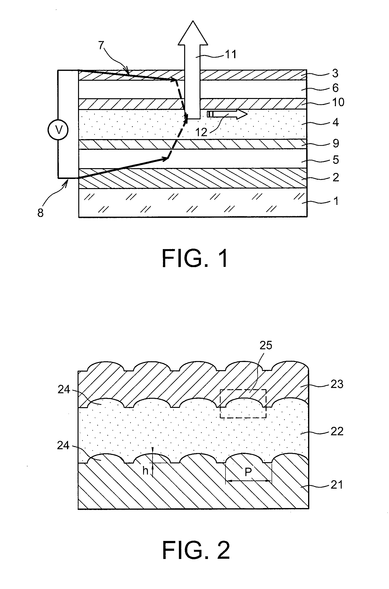
[0245]In this example, a substrate is prepared by the method according to the invention using a thermosetting resin, and then an organic light-emitting diode is prepared on said substrate by the method according to the invention.

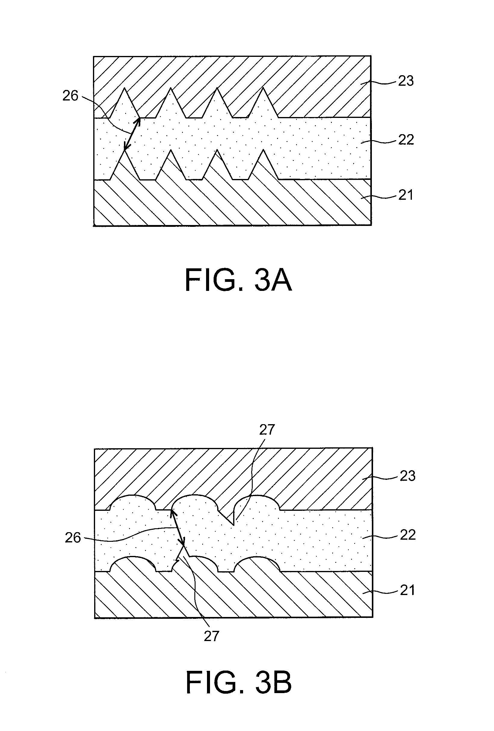
[0246]The method for preparing the substrate comprises the following successive steps:[0247]Deposition by PVD of the metal layer, for example in platinum or of a conducting layer with a thickness of 10 nm on the substrate;[0248]Deposition (or coating) of the commercially available thermosetting resin Neb® 22 of Sumito Chemical Japan on an 8 inch silicon wafer;[0249]Compression of the resin at 110° C. for 5 minutes under 300 mbars, by means of which a first nanostructuration is obtained which is a lattice of lines or a lattice of pads with a period from 200 nm to 600 nm and heights from 5 nm to 40 nm;[0250]After printing, plasma etching of the so-called residual resin layer which is present under the printed patterns in order to expose the substrate and the m...
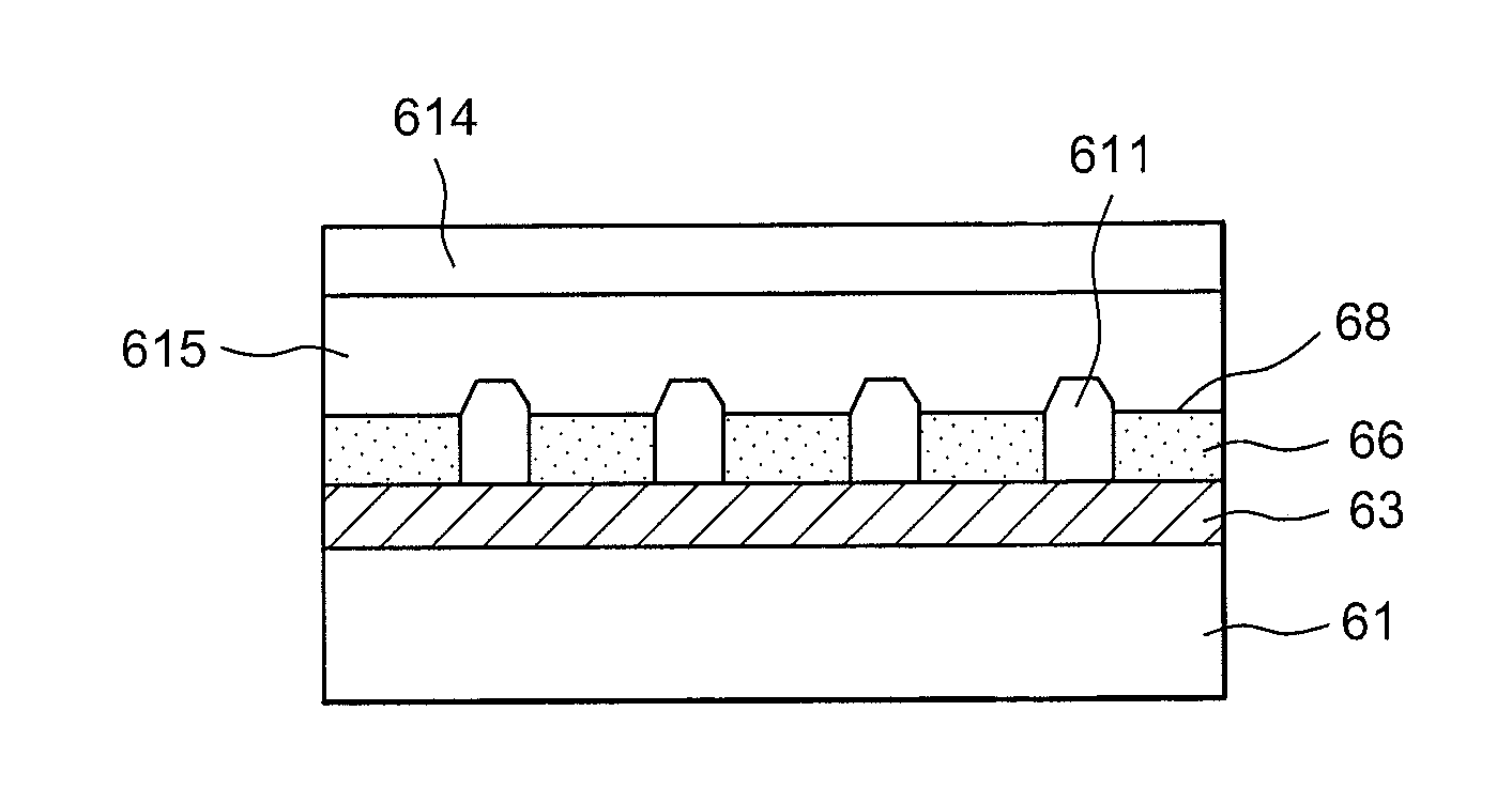
example 2

[0256]In this example, a conductive or metal layer for example in TIN is deposited on a substrate. Next, a dielectric material layer is deposited (for example a 100 nm layer of silicon dioxide).

[0257]On this dielectric layer, optical lithography is carried out (at a wave length of 193 nm) with a commercial resin such as a resin available at Rohm and Haas, Clariant or Tok, for making lattices of lines or holes, the periods of which range from 200 nm to 600 nm.

[0258]After developing the resin, the dielectric layer is etched right up to the level of the conductive layer by plasma or wet etching.

[0259]Next, the remaining resin is removed (stripped) so as to only leave the structured dielectric layer on the conductive layer.

[0260]Growth of the structures by electrochemistry in the thereby formed cavities is accomplished.

[0261]The produced patterns will have a height slightly larger than the height of the structures made in the dielectric layer in order to create a topography relative to ...


PUM

PropertyMeasurementUnit
heightaaaaaaaaaa
heightaaaaaaaaaa
heightaaaaaaaaaa

Abstract

A method for manufacturing an OLED and an electrode for an OLED, said electrode comprising a surface comprising a first dielectric nanostructuration and a second metal nanostructuration, on a substrate, wherein the following successive steps are carried out:a) a metal layer is deposited on a planar surface of a substrate;b) on the metal layer, a dielectric layer comprising said first dielectric nanostructuration which includes cavities which extend from the upper surface of the dielectric layer as far as the upper surface of the metal layer, is prepared;c) the cavities of the first dielectric nanostructuration are at least partially filled with a metal, whereby the second metal nanostructuration is obtained.

Description

TECHNICAL FIELD[0001]The invention relates to a method for manufacturing an electrode, preferably an anode, comprising a surface with metal and dielectric nanostructures for colored filtering and enhancement of light extraction in an Organic Light-Emitting Diode (OLED).[0002]The invention further relates to a method for manufacturing an organic light-emitting diode OLED comprising at least one step for manufacturing an electrode comprising a surface with metal and dielectric nanostructures with the above method.[0003]The technical field of the invention may be defined as that of organic light-emitting diodes and more particularly as that of organic light-emitting diodes for which one electrode, preferably the anode, is provided with metal nanostructurations with view to colored filtering and enhancement of the light extraction.STATE OF THE PRIOR ART[0004]Organic light-emitting diodes OLED are new generation diodes and are a very promising technology for displays, such as television ...

Claims


Application Information

Patent Timeline
Patent Type & Authority Applications(United States)
IPC IPC(8): H01L51/56
CPCH01L51/0023H01L51/5262H01L51/5203H10K71/621H10K50/805H10K50/85
Inventor LANDIS, STEFANCHAIX, NICOLASIVANOVA-HRISTOVA, VALENTINAPERNEL, CAROLE
Owner COMMISSARIAT A LENERGIE ATOMIQUE ET AUX ENERGIES ALTERNATIVES
Why Eureka
Try Eureka