Light emitting device with an omnidirectional photonic crystal

a light emitting device and photonic crystal technology, applied in the direction of solid-state devices, lasers, semiconductor lasers, etc., can solve the problems of significant increase in manufacturing costs and significant decrease in production yield, and achieve the effect of enhancing radiation extraction

Inactive Publication Date: 2005-07-14
HANSHIN CO LTD
View PDF3 Cites 35 Cited by
  • Summary
  • Abstract
  • Description
  • Claims
  • Application Information

AI Technical Summary

Benefits of technology

[0011] According to the present invention, there is provided a light emitting device that comprises: a light emitting diode that defines an upper outer surface and a lower outer surface opposite to the upper outer surface; and an omnidirectional photonic crystal formed on one of the upper outer surface and the lower outer surface of the light emitting diode and exhibiting a periodic variation in dielectric constant in such a manner so as to introduce an omnidirectional photonic band gap in a given frequency range such that the radiation generated by the light emitting diode in the frequency range for all incident angles and polarizations can be totally reflected by the omnidirectional photonic crystal, thereby enhancing radiation extraction from the other of the upper outer surface and the lower outer surface of the emitting diode, and that at least a portion of the radiation with frequencies outside the frequency range can pass through the omnidirectional photonic crystal.

Problems solved by technology

As a consequence, a light feedback apparatus is required to be used for transmitting the light to the detector, which results in a significant increase in the manufacturing cost.
Note that the cutting normally begins from the substrate side of the wafer, i.e., the back side of the wafer, in order to avoid damage to the semiconductor layers of the wafer (the LED dies tend to damage due to accumulated heat during cutting if the cutting begins from the semiconductor side of the wafer), which can result in a significant decrease in the production yield.

Method used


Image

  • Light emitting device with an omnidirectional photonic crystal
  • Light emitting device with an omnidirectional photonic crystal
  • Light emitting device with an omnidirectional photonic crystal

Examples


example 1

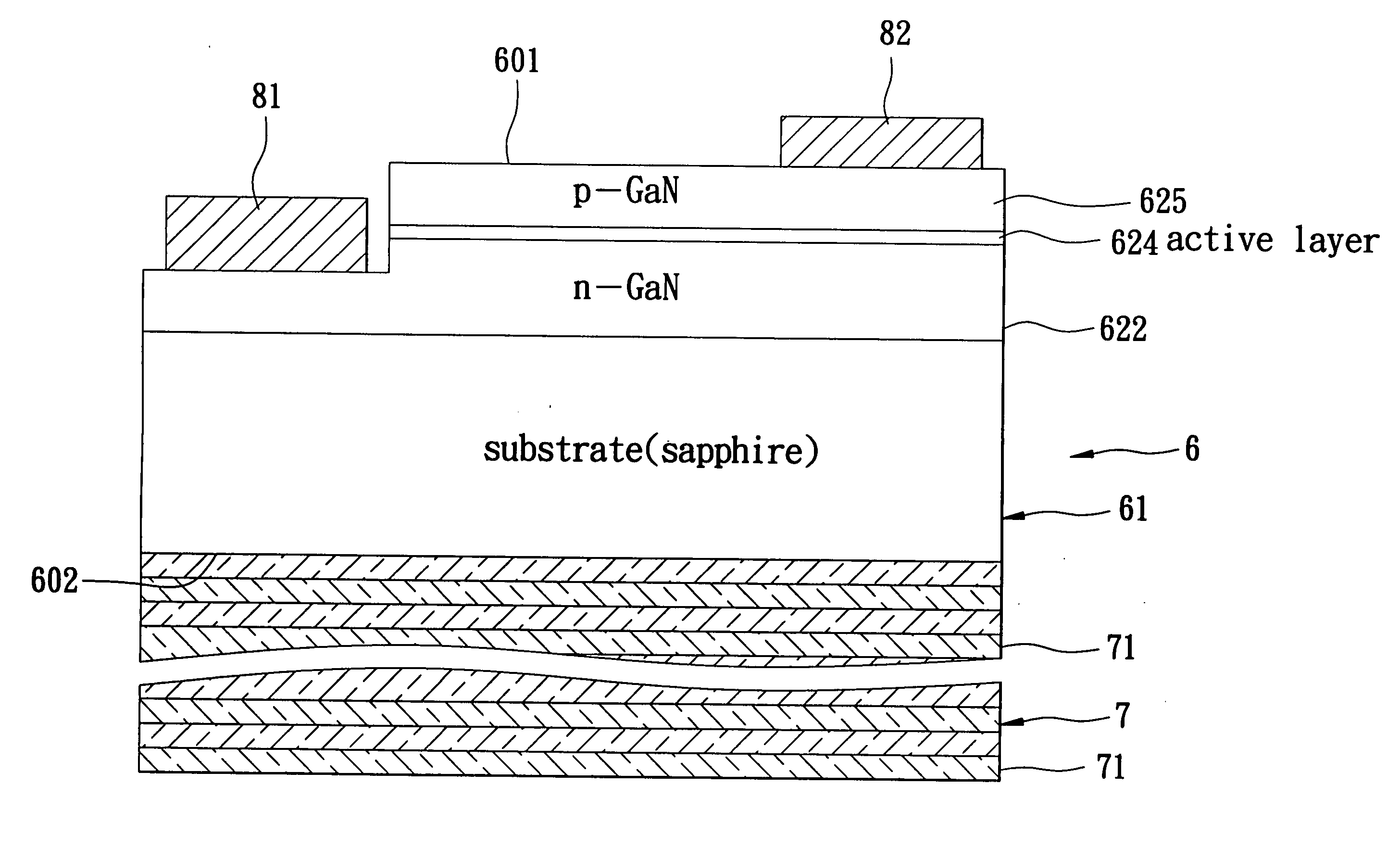
[0041] In this Example, the first and second semiconductor layers 622, 625 of the light emitting diode 6 are made from GaN material. The substrate 61 is made from sapphire. The light emitting diode 6 is capable of emitting a UV light radiation having a wavelength range ranging from 300 nm to 420 nm. The omnidirectional photonic crystal 7 is formed on the outer surface of the substrate 61 through e-beam evaporation techniques, and includes fourteen dielectric units 71, each of which includes the first and second dielectric layers 711, 712 which are respectively made from TiO2 and SiO2 and which respectively have refractive indices of 2.6 and 1.8, i.e., a refractive index difference of 1.12. The lattice constant a is equal to 110 nm. The thickness (d1) of the first dielectric layer 711 is equal to 0.42a.

[0042]FIG. 6 shows the presence of an omnidirectional photonic band gap in a frequency range between two dash lines in FIG. 6, i.e., between 0.273c / a and 0.3c / a, in the dispersion rel...

example 2

[0047] The light emitting device of this Example differs from the previous Example in that the light emitting diode 6 is capable of emitting a blue light radiation having a wavelength range ranging from 420 nm to 480 nm, that the thickness (d1) of the first dielectric layer 711 is equal to 0.42a, and that the first and second dielectric layers 711, 712 respectively have refractive indices of 2.42 and 1.47, i.e., a refractive index difference of 0.95. The lattice constant a is equal to 134 nm.

[0048]FIG. 11 shows the presence of an omnidirectional photonic band gap in a frequency range between two dash lines in FIG. 11, i.e., between 0.291c / a and 0.305c / a, in the dispersion relation of guided modes in a photonic band structure of the omnidirectional photonic crystal 7 of the light emitting device of Example 2.

[0049]FIGS. 12a and 12b illustrate variation of the band gap size of the omnidirectional photonic band gap as a function of the thickness (d1) of the first dielectric layer 711...

example 3

[0053] The light emitting device of this Example differs from the first Example in that the light emitting diode 6 is capable of emitting a green light radiation having a wavelength range ranging from 480 nm to 550 nm, that the thickness (d1) of the first dielectric layer 711 is equal to 0.45a, and that the first and second dielectric layers 711, 712 respectively have refractive indices of 2.36 and 1.46, i.e., a refractive index difference of 0.9. The lattice constant a is equal to 151 nm.

[0054]FIG. 16 shows the presence of an omnidirectional photonic band gap in a frequency range between two dash lines in FIG. 16, i.e., between 0.297c / a and 0.308c / a, in the dispersion relation of guided modes in a photonic band structure of the omnidirectional photonic crystal 7 of the light emitting device of Example 3.

[0055]FIGS. 17a and 17b illustrate variation of the band gap size of the omnidirectional photonic band gap as a function of the thickness (d1) of the first dielectric layer 711 (T...


PUM


Abstract

A light emitting device includes a light emitting diode and an omnidirectional photonic crystal formed on one of an upper outer surface and a lower outer surface of the light emitting diode and exhibiting a periodic variation in dielectric constant in such a manner so as to introduce an omnidirectional photonic band gap in a given frequency range such that the radiation generated by the light emitting diode in the frequency range for all incident angles and polarizations can be totally reflected by the omnidirectional photonic crystal, and that at least a portion of the radiation with frequencies outside the frequency range can pass through the omnidirectional photonic crystal.

Description

CROSS-REFERENCE TO RELATED APPLICATION [0001] This application claims priority of Taiwanese Application No. 093100473, filed on Jan. 8, 2004. BACKGROUND OF THE INVENTION [0002] 1. Field of the Invention [0003] This invention relates to a light emitting device including a light emitting diode and an omnidirectional photonic crystal formed on one of an upper outer surface and a lower outer surface of the light emitting diode. [0004] 2. Description of the Related Art [0005]FIG. 1 illustrates a conventional light emitting device 3 that includes a light emitting diode (LED) 12, and a Distributed Bragg Reflector (DBR) 14 embedded in the LED 12. The LED 12 includes a substrate 11, an n-type semiconductor layer 121, a p-type semiconductor layer 124, an active layer 123 sandwiched between the n-type and p-type semiconductor layers 121, 124, and n- and p-electrodes 122, 125 formed respectively on the n-type and p-type semiconductor layers 121, 124. The DBR 14 is sandwiched between the substra...

Claims


Application Information

Patent Timeline
Patent Type & Authority Applications(United States)
IPC IPC(8): H01L33/08H01L33/20H01L33/22H01L33/24H01L33/46H01S3/04H01S5/00
CPCH01L33/08H01L33/20H01L2933/0083H01L33/24H01L33/46H01L33/22H01L2224/16225
Inventor LIN, CHUNG-HSIANG
Owner HANSHIN CO LTD
Why Eureka
Try Eureka