Method of forming hole for interlayer connection conductor, method of producing resin substrate and component-incorporated substrate, and resin substrate and component-incorporated substrate

a technology of interlayer connection and hole, which is applied in the direction of sustainable manufacturing/processing, final product manufacturing, nuclear engineering, etc., can solve the problems of connection with interlayer connection conductor , quality problems, and inability to meet the requirements of interlayer connection, so as to improve quality and reduce cost , the effect of increasing the number of production steps

Active Publication Date: 2010-04-29
MURATA MFG CO LTD
View PDF11 Cites 10 Cited by
  • Summary
  • Abstract
  • Description
  • Claims
  • Application Information

AI Technical Summary

Benefits of technology

[0012]To overcome the problems described above, preferred embodiments of the present invention provide a method of forming a hole for an interlayer connection conductor that is suitable for producing a component-incorporated substrate, a resin substrate and a component-incorporated substrate having high quality in which a sufficient connection between an in-plane electrode and an interlayer connection conductor is produced at a low cost, and a resin substrate and a component-incorporated substrate that is produced without deformation of the interlayer connection conductor.
[0017]During machining a hole for an interlayer connection conductor on the resin layer using a laser beam, the in-plane electrode can be damaged by the laser beam when the surface of the in-plane electrode is rough or the thickness of the in-plane electrode is relatively small. In preferred embodiments of the present invention, since a light reflective conductor is formed on the in-plane electrode, a laser beam is reflected at the light reflective conductor, and damage to the in-plane electrode is effectively prevented. When a hole for an interlayer connection conductor is machined using a laser beam having a relatively large output, the light reflective conductor can be partially damaged. However, even in this case, damage to the in-plane electrode can be effectively prevented. Accordingly, an acceptable output range of the laser beam is increased. After machining a hole for an interlayer connection conductor, the hole is covered with or filled with a conductive material to form an interlayer connection conductor. At this time, the light reflective conductor functions to electrically connect the conductive material and the in-plane electrode, so that electrical reliability is improved.
[0018]Prior to the step of forming the light reflective conductor, a step of roughening the surface of the in-plane electrode may be performed. For the roughening step, a method of performing roughening after forming a pattern of the in-plane electrode on a base material, or a method of forming an electrode layer on a base material, roughening the entire electrode layer, and then forming an in-plane electrode by etching can be used, for example. The roughening step is preferably performed before the formation of a light reflective conductor. By roughening the surface of the in-plane electrode, adherence with the resin layer is improved.
[0021]In production of a component-incorporated substrate, it is preferable to conduct a second step of forming a light reflective conductor on the in-plane electrode, a third step of forming a mounting conductor for mounting a mount component on the in-plane electrode, and a fourth step of mounting a mount component on the in-plane electrode using the mounting conductor in the following manner. A mount component is mounted simultaneously with the formation of a light reflective conductor by applying a solder paste simultaneously in a region in which a light reflective conductor is to be formed (hereinafter, referred to as “light reflective conductor forming region”) and in a region in which a mounting conductor is to be formed (herein after referred to as “mounting conductor forming region”) on the in-plane electrode, and placing a mount component on the solder paste applied in the mounting conductor forming region, and simultaneously melting the solder pastes in the light reflective conductor forming region and in the mounting conductor forming region by heating. As a method of applying a solder paste, a known printing method may preferably be used, for example, and as a method of melting the solder paste by heating, a known reflow treatment may preferably be used, for example. In this case, since the formation of the light reflective conductor and the mounting of the mount component on the in-plane electrode (formation of a mounting conductor) can be simultaneously performed using the solder paste, there is no need to increase the number of production steps, and even a component-incorporated substrate having a large number of interlayer connection conductors can be produced at a low cost.
[0022]According to various preferred embodiments of the present invention, a high quality component-incorporated substrate in which sufficient connection between an in-plane electrode and an interlayer connection conductor is ensured can be produced at a low cost. In addition, a component-incorporated substrate can be produced without deformation of the interlayer connection conductor.

Problems solved by technology

However, ways to improve the quality and to reduce the cost thereof are problematic.
When a portion of the in-plane electrode 42 is removed and damaged, the connection with the interlayer connection conductor 48 is insufficient, and a quality problem arises.
This increases the cost, especially when a component-incorporated substrate having a large number of holes for the interlayer connection conductor 47 is produced.
However, when this method is used to produce a component-incorporated substrate, resin flow corresponding to the volume of the mount component occurs during the lamination of the resin layer, such that the hole for the interlayer connection conductor is likely to deform.
Therefore, the method disclosed in Japanese Unexamined Patent Publication No. 6-314884 is not suited for producing a component-incorporated substrate having a mount component incorporated therein.

Method used


Image

  • Method of forming hole for interlayer connection conductor, method of producing resin substrate and component-incorporated substrate, and resin substrate and component-incorporated substrate
  • Method of forming hole for interlayer connection conductor, method of producing resin substrate and component-incorporated substrate, and resin substrate and component-incorporated substrate
  • Method of forming hole for interlayer connection conductor, method of producing resin substrate and component-incorporated substrate, and resin substrate and component-incorporated substrate

Examples


first preferred embodiment

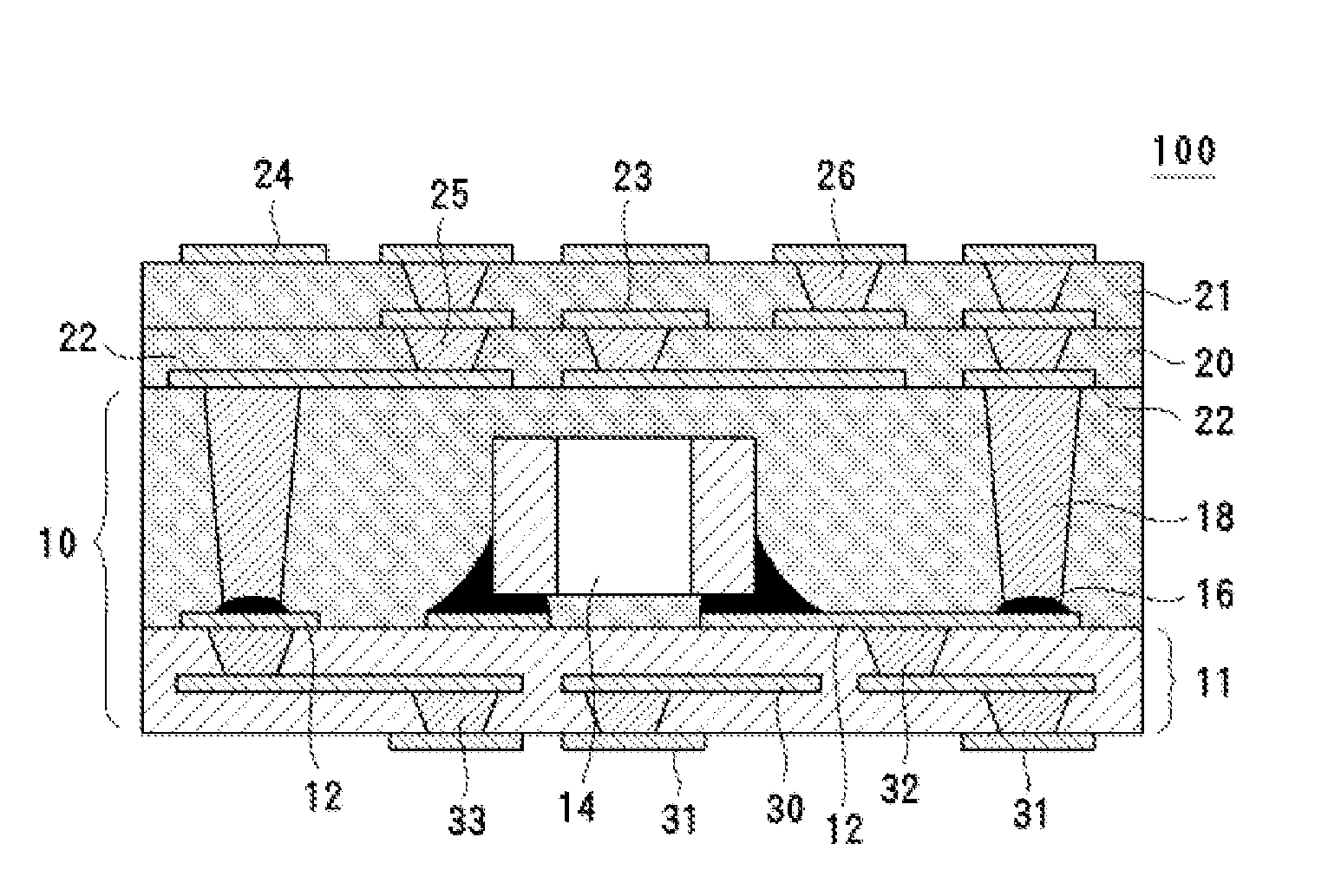
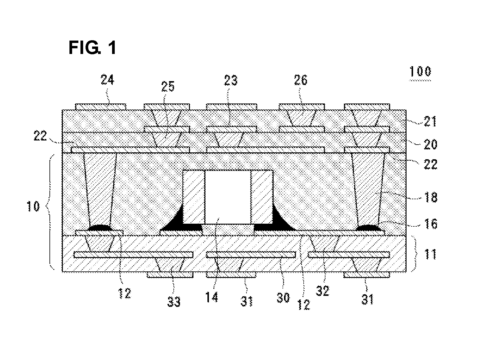
[0032]FIG. 1 is a longitudinal section of a component-incorporated module 100 formed by laminating a ceramic layer and a resin layer. In a component-incorporated substrate 10 which is a portion of the component-incorporated module 100, a mount component 14, such as a chip capacitor, for example, is mounted on a core substrate 11, and the top surface of the core substrate is provided with a resin layer 15 that covers the mount component 14. The top surface of the core substrate 11 includes an in-plane electrode 12, and the resin layer 15 includes an interlayer connection conductor (via conductor or through-hole conductor) 18. On the top surface of the component-incorporated substrate 10, other resin layers 20, 21 are laminated while in-plane electrodes 22, 23, 24 are interposed therebetween, and the in-plane electrode 12 is connected with the in-plane electrode 22 on the top surface of the resin layer 15 via the interlayer connection conductor 18. The in-plane electrodes 22, 23, 24 a...

second preferred embodiment

[0054]FIG. 4 shows another component-incorporated substrate 10A. This component-incorporated substrate 10A is produced using a transfer sheet instead of the core substrate 11, and transferring the in-plane electrode 12 to the resin layer 15 by peeling off the transfer sheet from the resin layer 15 after forming the resin layer 15 through the steps of FIGS. 2A to 2D and FIGS. 3A to 3C. As the transfer sheet, a metal sheet of stainless steel or other suitable material may be used, or a resin sheet, such as a carrier film, may be used. A metal foil may be pasted on the transfer sheet, and patterned to form an in-plane electrode. In this case, the component-incorporated substrate 10A is preferably made only of the resin layer 15, and the in-plane electrode 12 is exposed on the bottom surface of the resin layer 15.

third preferred embodiment

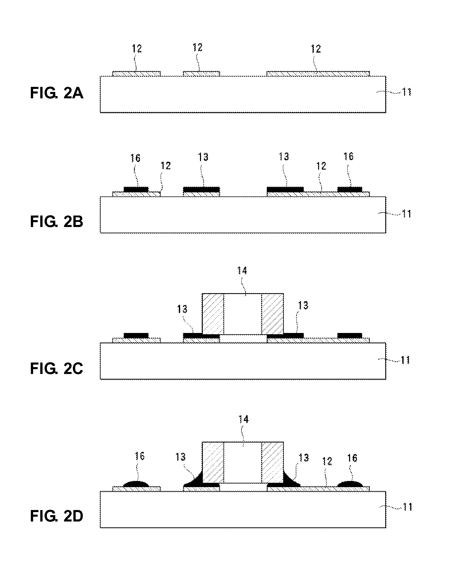
[0055]FIGS. 5A and 5B are views illustrating a method of roughening surface of the in-plane electrode 12. This roughening treatment is performed prior to the formation of the light reflective conductor 16 in the first preferred embodiment. As shown in FIG. 5A, the patterned in-plane electrode 12 is formed on the core substrate 11, and then an in-plane electrode 12a is roughened as shown in FIG. 5B. The roughening treatment is performed as either a dry method or a wet method, and the surface roughness Ra after the treatment is preferably about 1 μm, for example.

[0056]Steps following the roughening treatment are substantially the same as those of the first preferred embodiment. That is, after preparing the in-plane electrode 12a that is roughened as shown in FIG. 5B, the step of forming the light reflective conductor 16 and the mounting conductor 13, the step of mounting the mount component 14, the step of forming the resin layer 15, the step of forming the hole for the interlayer con...


PUM


Abstract

A high quality component-incorporated substrate achieves a sufficient connection between an in-plane electrode and an interlayer connection conductor at low cost. A method of forming a hole for an interlayer connection conductor of a resin substrate includes a step of forming an in-plane electrode in a core substrate, a step of forming a light reflective conductor for reflecting a laser beam applied on the in-plane electrode in a later step, a step of forming a resin layer so as to cover the core substrate, the in-plane electrode and the light reflective conductor, and a step of forming a hole for the interlayer connection conductor by removing the resin layer on the light reflective conductor through the use of a laser beam.

Description

BACKGROUND OF THE INVENTION[0001]1. Field of the Invention[0002]The present invention relates to a method of forming a hole for an interlayer connection conductor, a method of producing a resin substrate and a component-incorporated substrate, and a resin substrate and a component-incorporated substrate.[0003]2. Description of the Related Art[0004]A component-incorporated substrate in which a mount component is embedded inside a resin layer is lightweight and does not require burning at a high temperature as is the case with a ceramic multi-layer substrate, such that there are very few restrictions on the mount component to be incorporated therein. Therefore, such a component-incorporated substrate can be used in a wide variety of applications in the future. However, ways to improve the quality and to reduce the cost thereof are problematic.[0005]FIG. 7C illustrates a conventional component-incorporated substrate 40. In FIG. 7C, the component-incorporated substrate 40 includes a cor...

Claims


Application Information

Patent Timeline
Patent Type & Authority Applications(United States)
IPC IPC(8): H05K1/02H05K3/00
CPCH01L2924/01079H05K2203/043H05K3/244H01L2924/01046H05K3/3484H05K3/0035H05K1/187H05K2201/2054H05K2201/10636H05K3/4602H01L2924/09701H01L2224/82039H05K3/3442H05K3/20H01L2924/01004H01L2924/01078H05K3/3485Y02P70/50
Inventor SEKIMOTO, YASUYUKI
Owner MURATA MFG CO LTD
Why Eureka
Try Eureka