Substrate processing apparatus, substrate processing method, and computer readable storage medium

a substrate processing and substrate technology, applied in electrical apparatus, decorative surface effects, decorative arts, etc., can solve the problems of limited flexibility in designing a layout of the apparatus, device defects, and inability to reduce foot prints, so as to enhance the flexibility of designing a layout of the substrate processing apparatus.

Inactive Publication Date: 2010-04-29
TOKYO ELECTRON LTD
View PDF7 Cites 22 Cited by
  • Summary
  • Abstract
  • Description
  • Claims
  • Application Information

AI Technical Summary

Benefits of technology

[0025]According to the present invention, plural kinds of substrate storage shelves to be used for different storing purposes are integrated into one unit and aggregated in one place, an access position of a substrate transfer portion is shared for each of the substrate storage shelves, and the substrate storage shelves are moved to be in the access position. Therefore, because one appropriate position of the unit is determined by taking into consideration moving areas of the substrate storing shelves, designing flexibility of a layout of a substrate processing apparatus is enhanced and the designing is easily carried out, compared with a case where different kinds of the substrate storing shelves are separately arranged in different places and independently coupled to a transfer chamber.

Problems solved by technology

When the processed wafer W is transferred back to the load port 110, there may be a problem of so-called cross-contamination in which reaction products on the processed wafer W react with moisture in the atmosphere to produce a gas and this gas may be condensed on an unprocessed wafer W, thereby causing device defects.
However, because the substrate processing apparatus 100 so configured requires installing spaces for the storages 113, 116 depending on kinds of the storages, and the installing spaces and the number of the wafers to be stored are restricted due to an access area of the transfer arm, flexibility in designing a layout of the apparatus is limited and a foot print may not be reduced.
However, Patent document 1 does not describe a technology for storing plural kinds of wafers in the apparatus, or address an apparatus layout problem.

Method used


Image

  • Substrate processing apparatus, substrate processing method, and computer readable storage medium
  • Substrate processing apparatus, substrate processing method, and computer readable storage medium
  • Substrate processing apparatus, substrate processing method, and computer readable storage medium

Examples


first embodiment

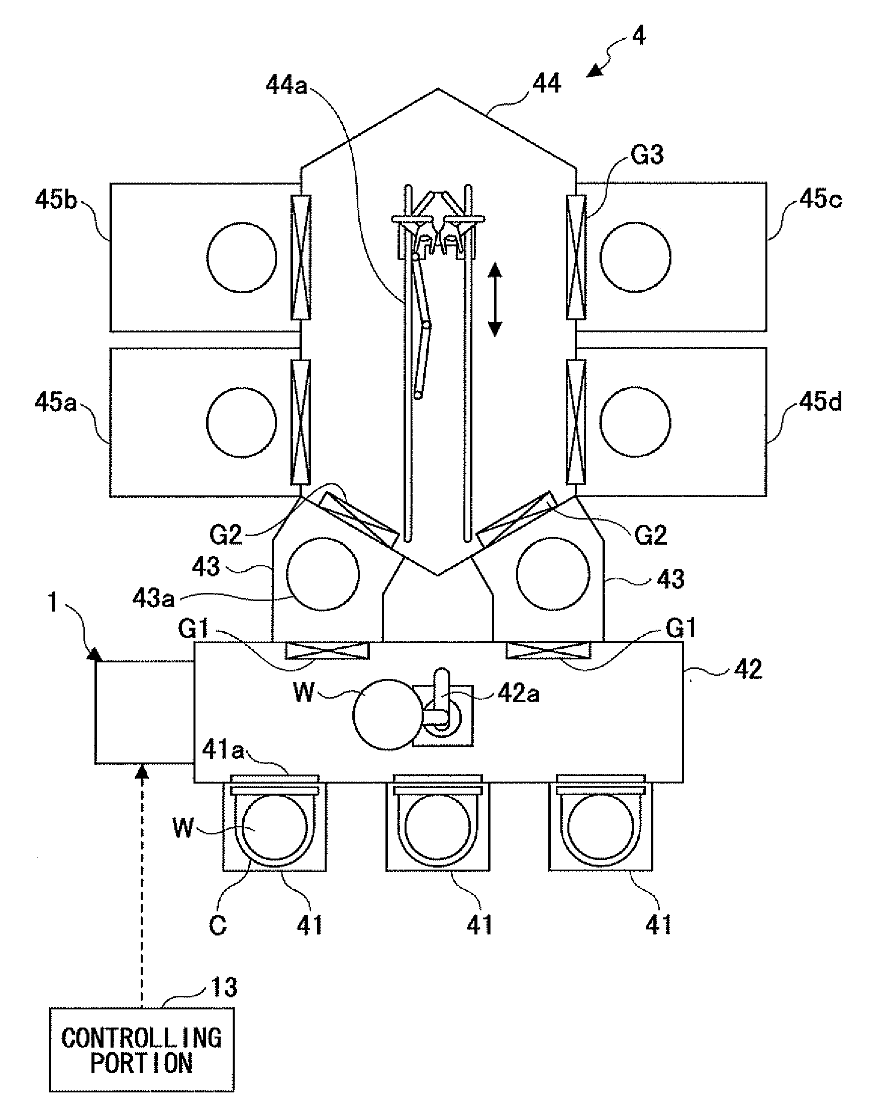
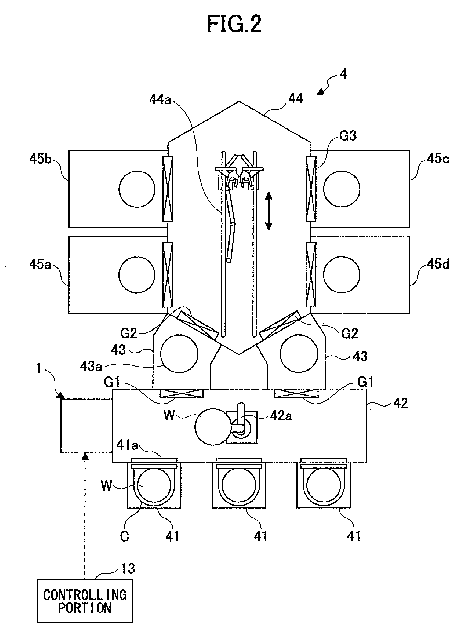
[0079]An entire configuration of a substrate processing apparatus according to an embodiment of the present invention is explained in the following. As shown in a plan view of FIG. 2, a substrate processing apparatus 4 is provided with a load port 41 for connecting a carrier C that houses the predetermined number of the wafers W to be processed to a main body of the substrate processing apparatus 4; a loader module 42 as a normal pressure transfer chamber in which the wafers W are transferred under a normal pressure aerial environment; two load lock chambers 43 whose inner space is switchable between a vacuum environment and a normal pressure aerial environment, and that hold the wafer W when the wafer W is transferred, the load lock chambers being arranged from side to side; a transfer module 44 as a vacuum transfer chamber in which the wafer W is transferred under a vacuum environment; and four processing modules 45a through 45d in which the wafer W transferred therein is processe...

second embodiment

[0106]Next, a substrate processing apparatus according to a second embodiment of the present invention is explained. The substrate processing apparatus according to the second embodiment is different in terms of the multi-storage unit from, and substantially the same in other configurations as the substrate processing apparatus according to the first embodiment. In the following, differences are mainly explained. FIG. 8 is a perspective view illustrating an inner configuration of a multi-storage unit 1a and FIG. 9 is a plan view of the inner configuration. In FIGS. 8 and 9, the same or similar reference numerals are given to the same or similar members or components as those in the substrate processing apparatus 4 according to the first embodiment, and repetitive explanations are omitted. Incidentally, the unit cover 11 of the substrate processing apparatus is removed in FIG. 8.

[0107]In the second embodiment, the purge storage 21 and the dummy storage 31 are integrally formed in lin...

third embodiment

[0110]Next, a substrate processing apparatus according to a third embodiment is explained. While, in the substrate processing apparatuses according to the first and the second embodiments, examples where the two kinds of storing shelves, i.e., the purge storage 21 and the dummy storage 31 are provided are explained, three or more kinds of storing shelves are provided in the third embodiment. FIG. 10 is a perspective view illustrating a multi-storage unit 1b of the substrate processing apparatus according to the third embodiment, and FIG. 11 is a plan view of the multi-storage unit 1b. In addition, FIG. 12 is a perspective view of a rotating member 5 inside the multi-storage unit 1b. In FIGS. 10 through 12, the same or similar reference numerals are given to the same or similar members or parts as those in the first and the second embodiments, and repetitive explanations are omitted.

[0111]As shown in FIGS. 10, 11, the multi-storage unit 1b according to the third embodiment has substa...


PUM

PropertyMeasurementUnit
traverse widthaaaaaaaaaa
areaaaaaaaaaaa
vacuum environmentaaaaaaaaaa

Abstract

A substrate processing apparatus is disclosed for bringing a substrate from a carrier, by a substrate transfer portion inside a transfer chamber, into a processing module to perform a process therein. The substrate processing apparatus includes a substrate storing chamber coupled to an exterior of the transfer chamber via a transfer opening to be in communications with the transfer chamber; a first storing shelf in the substrate storing chamber to store substrates for a first storing purpose; a second storing shelf in the substrate storing chamber to store substrates for a second storing purpose different from the first storing purpose; and a shifting mechanism that shifts the first and the second storing shelves to position a substrate storing area of one of the first and the second storing shelves so that substrate transferring is enabled between the substrate storing area and the substrate transfer portion via the transfer opening.

Description

TECHNICAL FIELD[0001]The present invention relates to a substrate processing apparatus that carries out a substrate process in a processing module, and specifically to a technology for storing a wafer in the processing apparatus for different purposes.BACKGROUND ART[0002]In semiconductor device manufacturing, there is an operation in which a vacuum process such as an etching process and the like is carried out on a substrate to be processed, for example, a semiconductor wafer (referred to as a wafer, hereinafter). In order to carry out such a process at a high throughput, a vacuum processing apparatus called a multi-chamber system and the like is used.[0003]Among the vacuum processing apparatuses, one having a vacuum processing chamber and an atmospheric transfer chamber has been known. An example of such a vacuum processing apparatus is shown in FIG. 1. A vacuum processing apparatus 100 is composed of a load port 110 provided with a stage on which a carrier C such as a Front Openin...

Claims


Application Information

Patent Timeline
Patent Type & Authority Applications(United States)
IPC IPC(8): C23F1/00C23F1/08
CPCH01L21/67778H01L21/67769
Inventor KONDOH, KEISUKE
Owner TOKYO ELECTRON LTD
Why Eureka
Try Eureka