Electroluminescent display with efficiency compensation

a technology of efficiency compensation and electroluminescent display, which is applied in the direction of electroluminescent light sources, static indicating devices, instruments, etc., can solve the problems of reducing the lifetime of the display, differential color aging, and a display whose display life, and achieves the effect of simple voltage measurement circuitry

Active Publication Date: 2010-04-29
GLOBAL OLED TECH
View PDF17 Cites 30 Cited by
  • Summary
  • Abstract
  • Description
  • Claims
  • Application Information

AI Technical Summary

Benefits of technology

[0026]An advantage of this invention is an electroluminescent display, such as an OLED display, that compensates for the aging of the organic materials in the display wherein circuitry or transistor aging or nonuniformities are present, without requiring extensive or complex circuitry for accumulating a continuous measurement of light-emitting element use or time of operation. It is a further advantage of this invention that it uses simple voltage measurement circuitry. It is a further advantage of this invention that by making all measurements of voltage, it is more sensitive to changes than methods that measure current. It is a further advantage of this invention that a single select line can be used to enable data input and data readout. It is a further advantage of this invention that characterization and compensation of OLED changes are unique to the specific element and are not impacted by other elements that may be open-circuited or short-circuited.

Problems solved by technology

However, as the display is used, the organic materials in the display age and become less efficient at emitting light.
This reduces the lifetime of the display.
The differing organic materials can age at different rates, causing differential color aging and a display whose white point varies as the display is used.
In addition, each individual pixel can age at a rate different from other pixels, resulting in display nonuniformity.
This technique has the disadvantage of not representing the performance of small-molecule organic light emitting diode displays well.
Also, this technique does not accommodate differences in behavior of the display at varying levels of brightness and temperature and cannot accommodate differential aging rates of the different organic materials.
This technique requires the measurement and accumulation of drive current applied to each pixel, requiring a stored memory that must be continuously updated as the display is used, and therefore requiring complex and extensive circuitry.
However, this technique is only applicable to passive-matrix displays, not to the higher-performance active-matrix displays which are commonly employed.
Further, this technique does not include any correction for changes in OLED emitters as they age, such as OLED efficiency loss.
This design requires the use of a calculation unit responsive to each signal sent to each pixel to record usage, greatly increasing the complexity of the circuit design.
This design presumes a predictable relative use of pixels and does not accommodate differences in actual usage of groups of pixels or of individual pixels.
Hence, correction for color or spatial groups is likely to be inaccurate over time.
This integration is complex, reduces manufacturing yields, and takes up space within the display.
The measurement techniques are iterative, and therefore slow.
However, drive transistors known in the art have non-idealities that are confounded with the OLED emitter aging in this method.
The method of Arnold et al. will therefore not provide complete compensation for OLED efficiency losses in circuits wherein transistors show such effects.
Additionally, when methods such as reverse bias are used to mitigate a-Si transistor threshold voltage shifts, compensation of OLED efficiency loss can become unreliable without appropriate and potentially expensive tracking and prediction of reverse bias effects.

Method used


Image

  • Electroluminescent display with efficiency compensation
  • Electroluminescent display with efficiency compensation
  • Electroluminescent display with efficiency compensation

Examples


Embodiment Construction

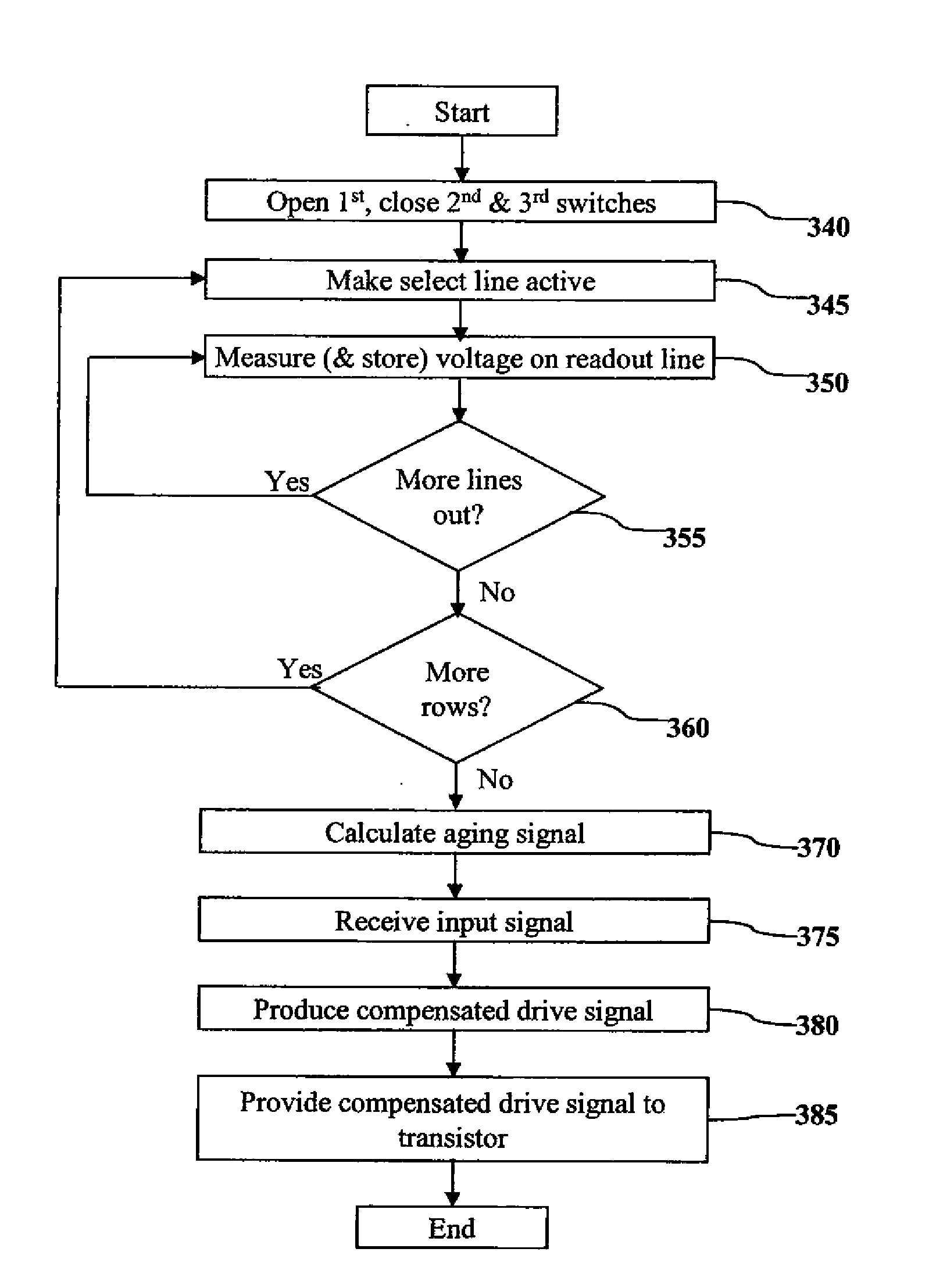
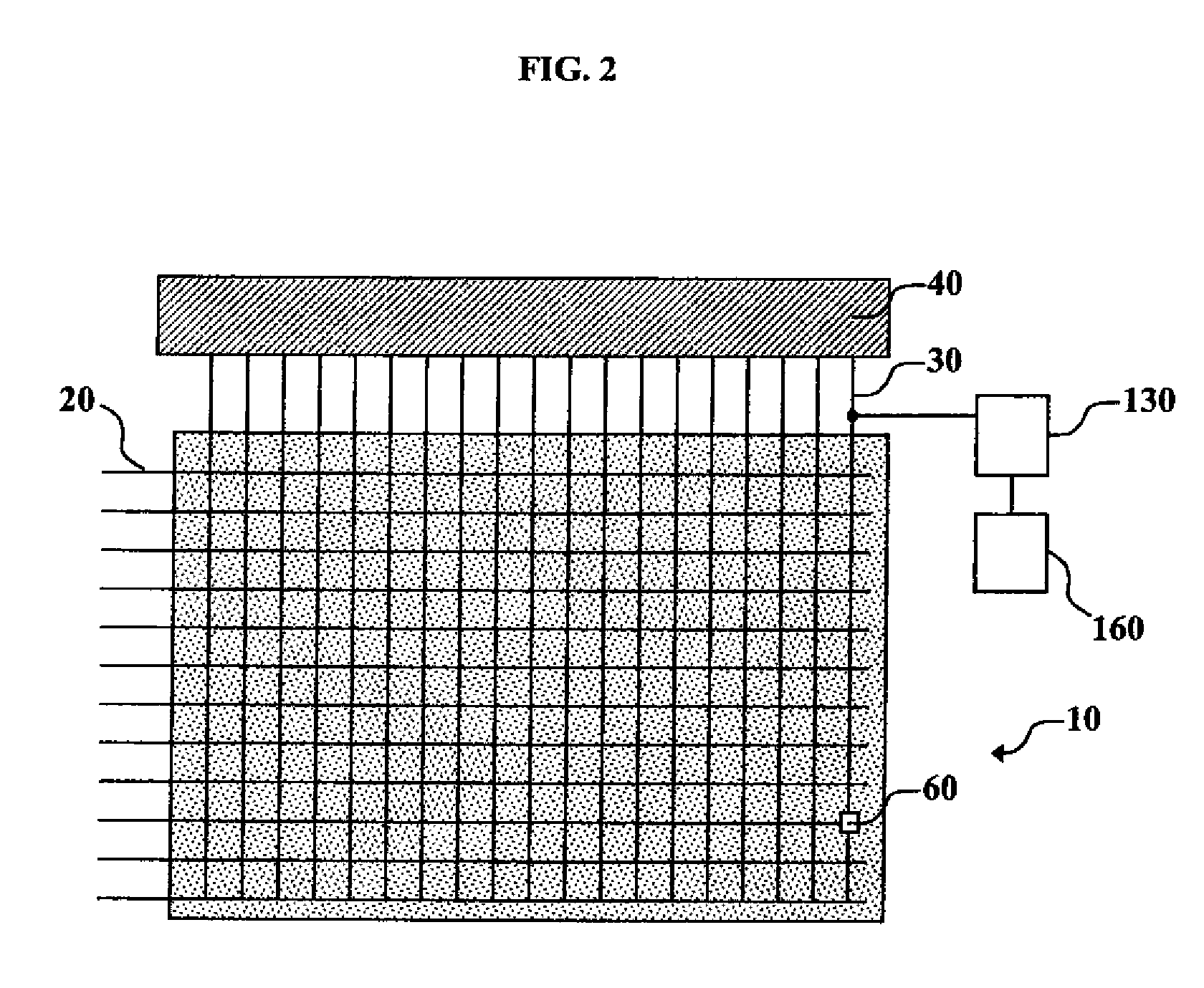
[0034]Turning now to FIG. 2, there is shown a schematic diagram of one embodiment of an electroluminescent (EL) display that can be used in the practice of the present invention. EL display 10 comprises an array of a predetermined number of EL subpixels 60 arranged in rows and columns. EL display 10 includes a plurality of row select lines 20 wherein each row of EL subpixels 60 has a row select line 20. EL display 10 includes a plurality of readout lines 30 wherein each column of EL subpixels 60 has a readout line 30. Each readout line 30 is connected to a third switch 130, which selectively connects readout line 30 to current source 160 during the calibration process Although not shown for clarity of illustration, each column of EL subpixels 60 also has a data line as is well-known in the art. The plurality of readout lines 30 is connected to one or more multiplexers 40, which permits parallel / sequential readout of signals from EL subpixels, as will become apparent. Multiplexer 40 ...


PUM


Abstract

An electroluminescent (EL) subpixel having a readout transistor is driven by a current source when the drive transistor is non-conducting. This produces an emitter-voltage signal from which an aging signal representing the efficiency of the EL emitter can be computed. The aging signal is used to adjust an input signal to produce a compensated drive signal to compensate for changes in efficiency of the EL emitter.

Description

CROSS REFERENCE TO RELATED APPLICATIONS[0001]Reference is made to commonly-assigned, co-pending US Patent Application U.S. Ser. No. 11 / 766,823 entitled “OLED Display with Aging and Efficiency Compensation” by Levey et al, dated Jun. 22, 2007, incorporated by reference herein.FIELD OF THE INVENTION[0002]The present invention relates to solid-state electroluminescent flat-panel displays and more particularly to such displays having ways to compensate for efficiency loss of the electroluminescent display components.BACKGROUND OF THE INVENTION[0003]Electroluminescent (EL) devices have been known for some years and have been recently used in commercial display devices. Such devices employ both active-matrix and passive-matrix control schemes and can employ a plurality of subpixels. Each subpixel contains an EL emitter and a drive transistor for driving current through the EL emitter The subpixels are typically arranged in two-dimensional arrays with a row and a column address for each su...

Claims


Application Information

Patent Timeline
Patent Type & Authority Applications(United States)
IPC IPC(8): G06F3/038H05B44/00
CPCG09G3/3233G09G2300/0819G09G2310/0297G09G2320/0693G09G2320/0295G09G2320/043G09G2320/045G09G2320/0233G09G3/32H05B33/02G09G3/30
Inventor LEON, FELIPE A.
Owner GLOBAL OLED TECH
Why Eureka
Try Eureka