Power line decoding method for an memory array

Inactive Publication Date: 2010-04-29
SEMICON MFG INT (SHANGHAI) CORP
View PDF6 Cites 18 Cited by
  • Summary
  • Abstract
  • Description
  • Claims
  • Application Information

AI Technical Summary

Benefits of technology

[0013]Numerous benefits are achieved using one or more features of the present invention. In a specific embodiment, the present invention can provide an SRAM array having reduced standby current by lowering the power supply voltage of inactive cells. In certain embodiments, the invention can provide full power supply to active memory cells to maintain operating speed of the memory array. Certain embodiments of the invention achieve simple design and l

Problems solved by technology

An IC fabrication facility can cost hundreds of millions, or even billions, of dollars.
Making devices smaller is very challenging, as each process used in IC fabrication has a limit.
An example of such a limit is that memory cell standby current has become an major contributor to overall integrated circuits power consumption.
Although fabless chip companies and foundry ser

Method used


Image

  • Power line decoding method for an memory array
  • Power line decoding method for an memory array
  • Power line decoding method for an memory array

Examples


Example

[0025]According to the present invention, techniques directed to integrated circuits and their processing are provided for the manufacture of semiconductor devices. More particularly, the invention provides a method and device for selectively lowering power supply voltage to an SRAM memory array. Merely by way of example, the invention has been applied to SRAM devices for providing low power consumption while maintaining high memory speed. But it would be recognized that the invention has a much broader range of applicability. For example, the invention can be applied to other embedded or stand-alone integrated circuits memories, such as DRAM and non-volatile memories.

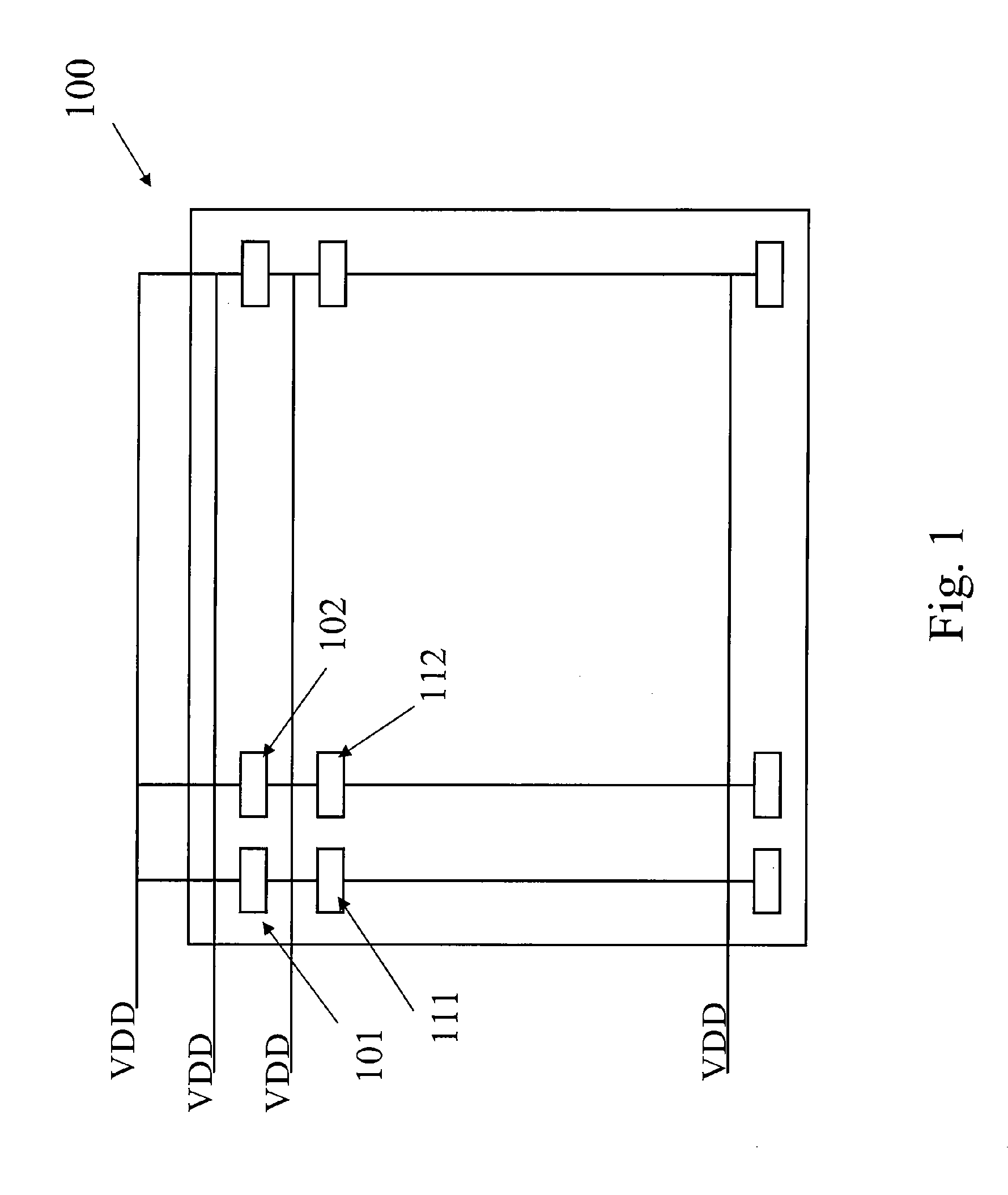
[0026]FIG. 1 is a schematic diagram of a conventional SRAM array 100. As shown SRAM memory array 100 includes memory cells, such as 101, 102, . . . , 111, 112, . . . , etc. In a typical conventional SRAM array, such as 100, all memory cells are supplied with the same power supply voltage VDD. The power grid in the arra...


PUM


Abstract

A method for selectively providing power supply voltage to a memory device. The method provides an integrated circuit memory device including a first plurality of memory cells. Each memory cell includes a power terminal and a ground terminal. The method includes selecting a second plurality of memory cells from the first plurality of memory cells. The method provides a first power voltage to the power terminal of each of the selected memory cells and a second power voltage to the power terminal of each of the unselected memory cells. The second power voltage is lower than the first power voltage. In an embodiment, the method applies a first ground voltage to the ground terminal of each of the selected memory cells and applies a second ground voltage to the ground terminal of each of the unselected memory cells. The second ground voltage is higher than the first ground voltage.

Description

CROSS-REFERENCES TO RELATED APPLICATIONS[0001]This application claims priority to Chinese Patent Application No. 200810201786.8, filed Oct. 24, 2008, commonly assigned, incorporated by reference herein for all purposes.BACKGROUND OF THE INVENTION[0002]The present invention is directed to integrated circuits and their processing for the manufacture of semiconductor devices. More particularly, the invention provides a method and device for selectively lowering power supply voltage to an SRAM memory array. Merely by way of example, the invention has been applied to SRAM devices for providing low power consumption while maintaining high memory speed. But it would be recognized that the invention has a much broader range of applicability. For example, the invention can be applied to other embedded or stand-alone integrated circuits memories, such as DRAM and non-volatile memories.[0003]Integrated circuits or “ICs” have evolved from a handful of interconnected devices fabricated on a sing...

Claims


Application Information

Patent Timeline
IPC IPC(8): G11C5/14
CPCG11C5/147G11C11/413G11C11/412
Inventor OUYANG, PAULLI, ZHIHUANG, QIANG
Owner SEMICON MFG INT (SHANGHAI) CORP
Why Eureka
Try Eureka