Verification of array built-in self-test (ABIST) design-for-test/design-for-diagnostics (dft/dfd)

a self-testing and array technology, applied in the field of vlsi device testing, can solve the problem of not providing a means to adequately detect all of the internal defects of the devi

Active Publication Date: 2010-05-06
SIEMENS PROD LIFECYCLE MANAGEMENT SOFTWARE INC
View PDF15 Cites 7 Cited by
  • Summary
  • Abstract
  • Description
  • Claims
  • Application Information

AI Technical Summary

Problems solved by technology

One of the problems with semiconductor test techniques is associated with the usage of automatic test equipment (ATE) to apply the test patterns at the device's external inputs and measure the responses at the device's external outputs.
This approach does not provide a means to adequately detect all of the device's internal defects.
If the Flush and Scan tests fail, no further testing is required in a particular test mode or chip configuration, since all subsequent LSSD tests would also fail, therefore, a typical manufacturing test flow would skip out at that point.

Method used


Image

  • Verification of array built-in self-test (ABIST) design-for-test/design-for-diagnostics (dft/dfd)
  • Verification of array built-in self-test (ABIST) design-for-test/design-for-diagnostics (dft/dfd)
  • Verification of array built-in self-test (ABIST) design-for-test/design-for-diagnostics (dft/dfd)

Examples


Embodiment Construction

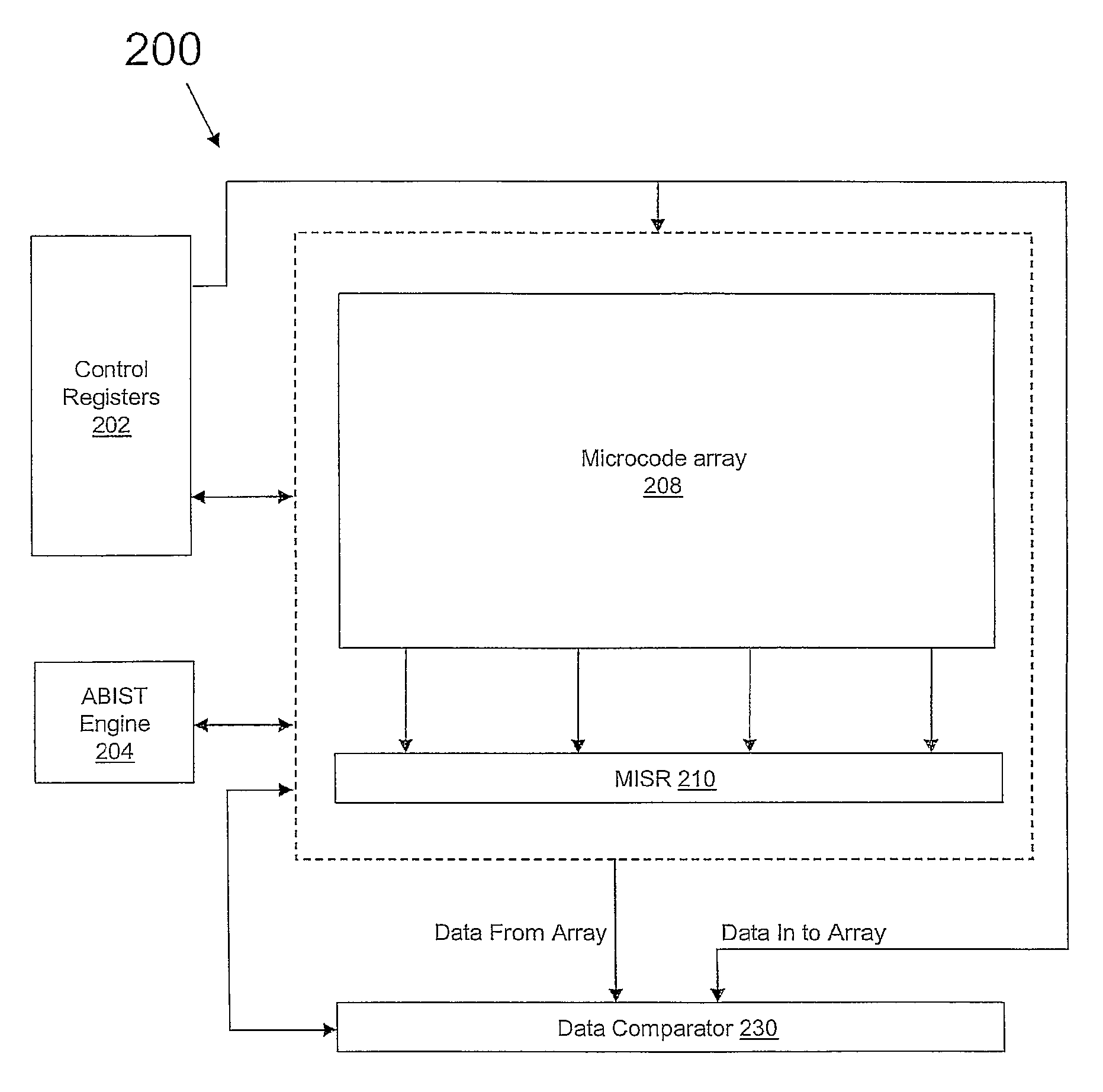
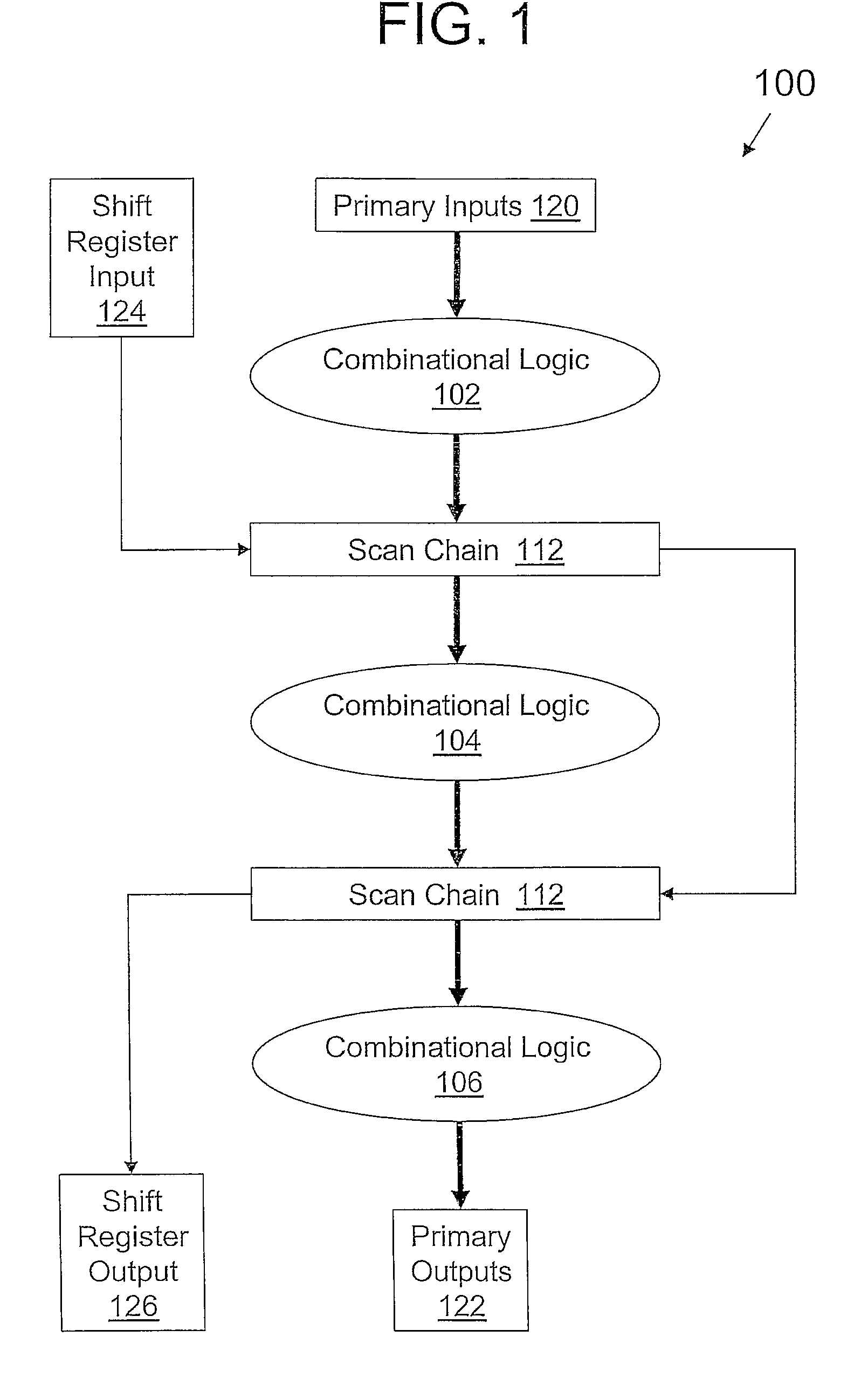
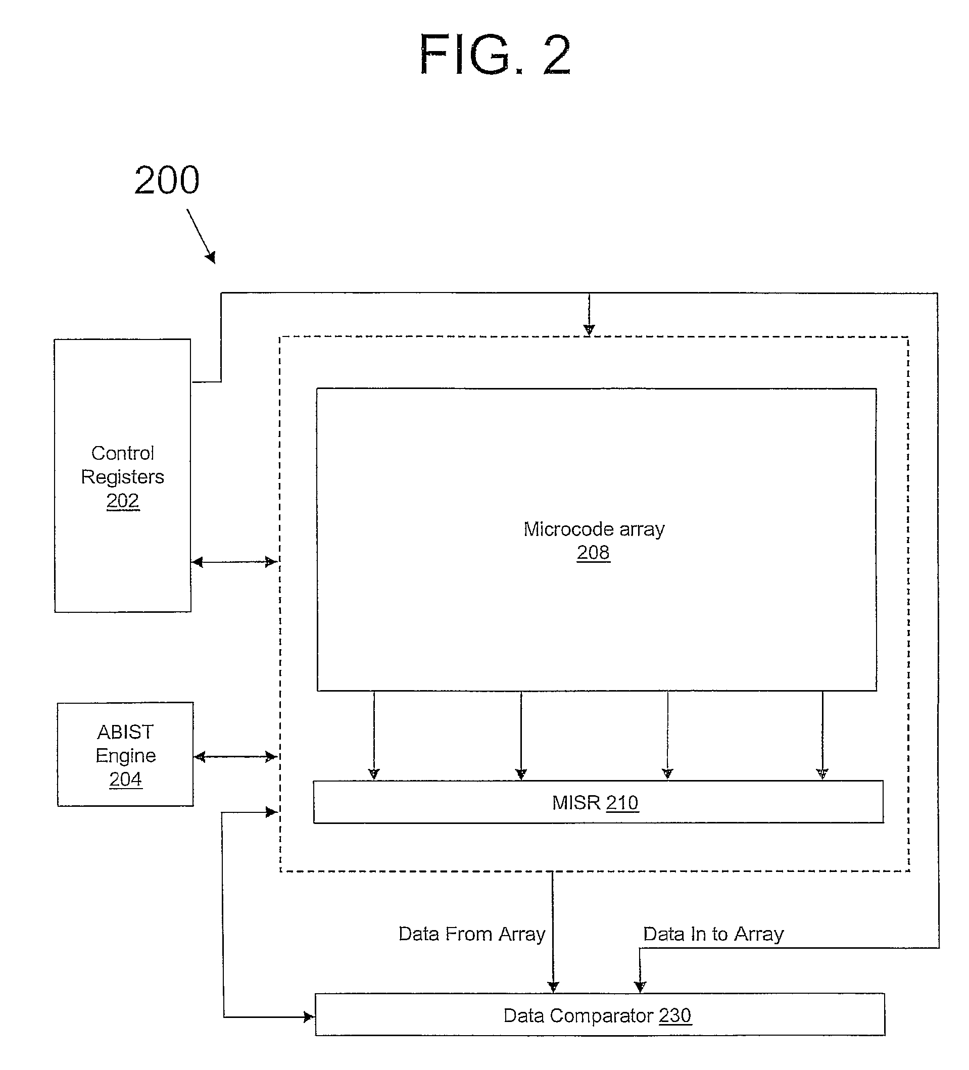
[0007]Disclosed is a method, system and computer program product for testing the Design-For-Testability / Design-For-Diagnostics (DFT / DFD) and supporting BIST structures and functions of a custom microcode array. Upon completion of the LSSD Flush and Scan tests, a LSSD test of the DFT functional combinational logic is performed by applying generated LSSD deterministic test patterns targeting the ABIST design-for-test to determine if the DFT supporting the microcode array is functioning correctly. Additional tests may be terminated upon resulting failure of the applied ABIST DFT circuitry surrounding the arrays.

[0008]The above as well as additional features and advantages of the present invention will become apparent in the following detailed written description.

BRIEF DESCRIPTION OF THE DRAWINGS

[0009]The invention itself will best be understood by reference to the following detailed description of an illustrative embodiment when read in conjunction with the accompanying drawings, where...


PUM


Abstract

A method, system and computer program product for testing the Design-For-Testability / Design-For-Diagnostics (DFT / DFD) and supporting BIST functions of a custom microcode array. Upon completion of the LSSD Flush and Scan tests, the ABIST program is applied to target the logic associated direct current (DC) and alternating current (AC) faults of ABIST array Design-For-Testability / Design-For-Diagnostics DFT / DFD functions that support the microcode array. A LSSD test of the DFT functional combinational logic is performed by applying generated LSSD deterministic test patterns targeting the ABIST design-for-test faults to determine if the DFT supporting the microcode array is functioning correctly. Additional tests may be terminated upon resulting failure of the applied ABIST DFT circuitry surrounding the arrays.

Description

BACKGROUND[0001]1. Technical Field[0002]The present invention generally relates to VLSI device testing in general, and in particular to testing the Design-For-Testability / Design-For-Diagnostics (DFT / DFD) and supporting built-in self-test (BIST) structures and functions of a custom microcode array.[0003]2. Description of the Related Art[0004]One of the problems with semiconductor test techniques is associated with the usage of automatic test equipment (ATE) to apply the test patterns at the device's external inputs and measure the responses at the device's external outputs. This approach does not provide a means to adequately detect all of the device's internal defects. Direct access to the internal structures of a device is necessary. This need has led to the development of design-for-test (DFT) and array built-in self-test (ABIST) techniques and methods.[0005]DFT techniques include design rules and constraints aimed at increasing the testability of a design through increased intern...

Claims


Application Information

Patent Timeline
Patent Type & Authority Applications(United States)
IPC IPC(8): G06F11/07
CPCG01R31/318544G06F11/2236G11C29/16G11C29/32G11C2029/3202
Inventor FORLENZA, DONATO ORAZIOFORLENZA, ORAZIO PASQUALEROBBINS, BRYAN J.TRAN, PHONG T.
Owner SIEMENS PROD LIFECYCLE MANAGEMENT SOFTWARE INC
Why Eureka
Try Eureka