Integrated Leadframe And Bezel Structure And Device Formed From Same

a leadframe and bezel technology, applied in the direction of solid-state devices, basic electric elements, instruments, etc., can solve the problems of reducing the size of the completed structure, the need to keep the fingers relatively still, and the number of components, so as to achieve the effect of enhancing the overall package size, enhancing conductivity, and enhancing the resistance to wear and corrosion

Inactive Publication Date: 2010-05-27
APPLE INC
View PDF9 Cites 92 Cited by
  • Summary
  • Abstract
  • Description
  • Claims
  • Application Information

AI Technical Summary

Benefits of technology

[0018]According to one aspect of the invention, an integrated leadframe and bezel structure is disclosed. This integrated leadframe and bezel may be stamped, etched, etc. from sheet material such as copper, copper alloy, or the like in a manner similar to that by which known IC leadframes are currently formed. The layout and dimensions of the leadframe are selected such that one or more portions of the leadframe may be bent out of the plane of the sheet to create bezel region(s). This bending may be accomplished by die-stamping or other process for rapid, automated fabrication.
[0021]According to a yet further aspect of the present invention, the bezel region(s) is formed to have a resiliently deformable support. Once bent into position, the bezel may then move up and down relative to the upper surface of the sensor IC mounted to the die pad of the leadframe. The relative positions of the planes of the bezel and the upper surface of the sensor IC may then be controlled, for example with the upper surface of the sensor IC as the reference plane and the bezel moving up or down relative thereto, to obtain the desired displacement between the two planes. This provides control over the relative area and / or force applied by a fingertip as between the bezel and the sensor IC.
[0022]According to a still further aspect of the present invention, the bezel region(s) is at least as wide as the width of the sensor structure formed in the sensor IC. Contact area between the user's finger and the bezel surface is therefor maximized without increasing the size of the overall package.
[0023]According to yet another aspect of the present invention, regions of the integrated leadframe and bezel may be selectively plated, for example to enhance conductivity, provide environmental protection, etc. In one embodiment, the bezel region(s) are plated, for example with Ni—Sn, so as to provide a conductive surface with enhanced resistance to wear, corrosion, etc. due to the exposure of the bezel region(s) to atmosphere, friction (finger swipe), oils (from the fingertip), etc.

Problems solved by technology

Indeed, the finger must be kept relatively motionless during the sensing phase to obtain undistorted results.
However, as in the general art of IC production, there is significant, ongoing commercial pressure to reduce cost, number of components, and number and complexity of manufacturing steps, and size of the completed structure.

Method used


Image

  • Integrated Leadframe And Bezel Structure And Device Formed From Same
  • Integrated Leadframe And Bezel Structure And Device Formed From Same
  • Integrated Leadframe And Bezel Structure And Device Formed From Same

Examples


Embodiment Construction

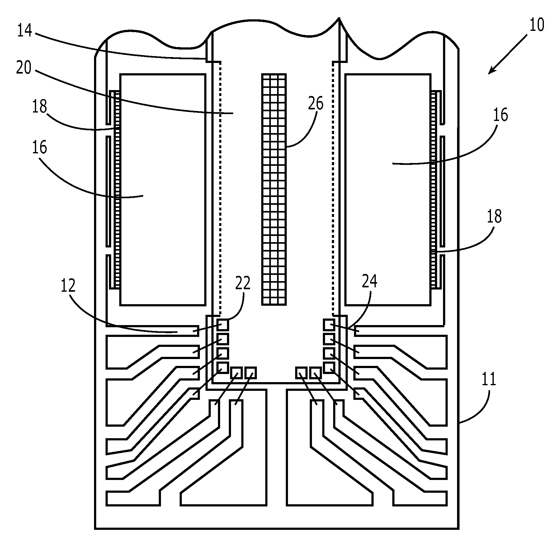
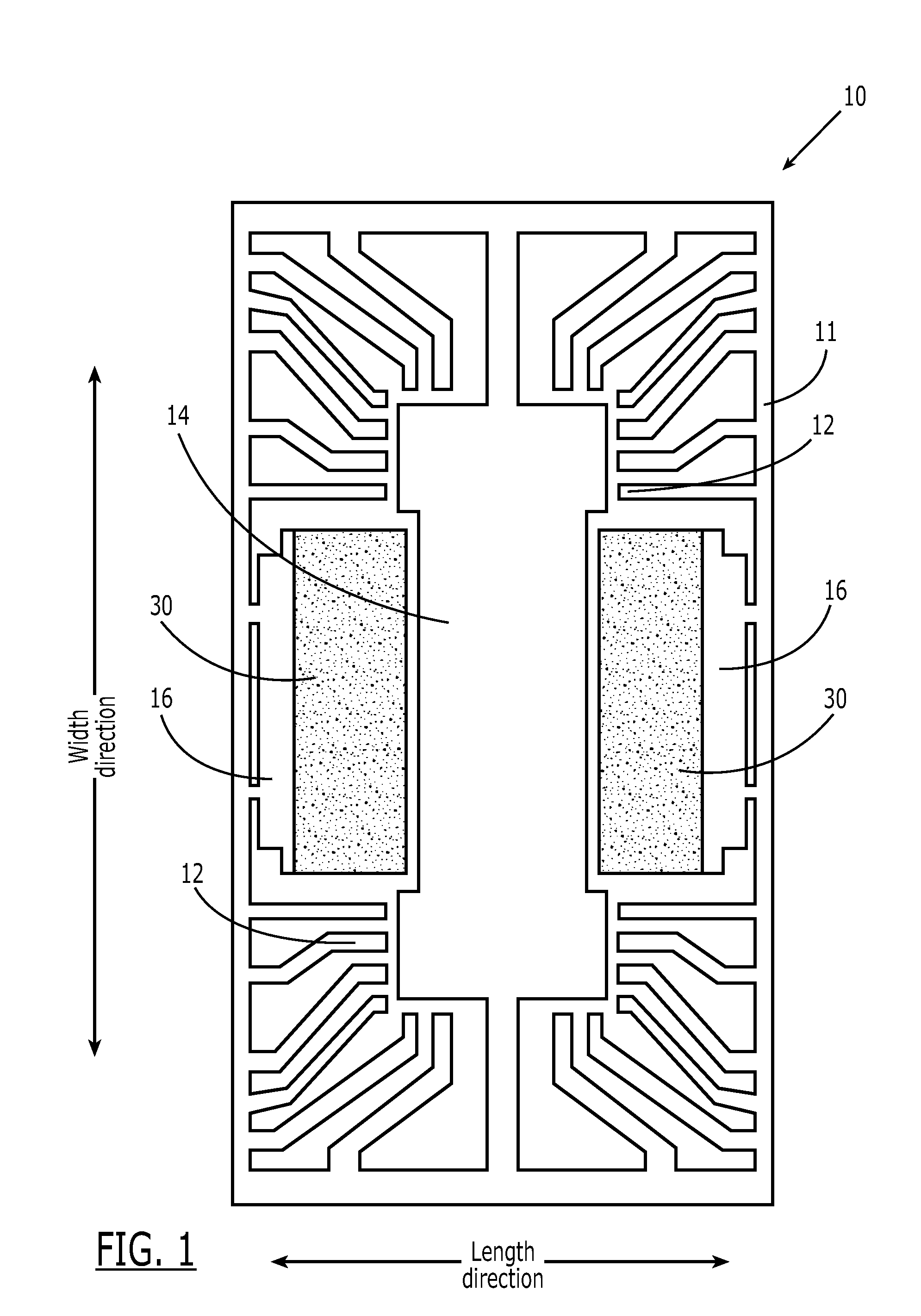
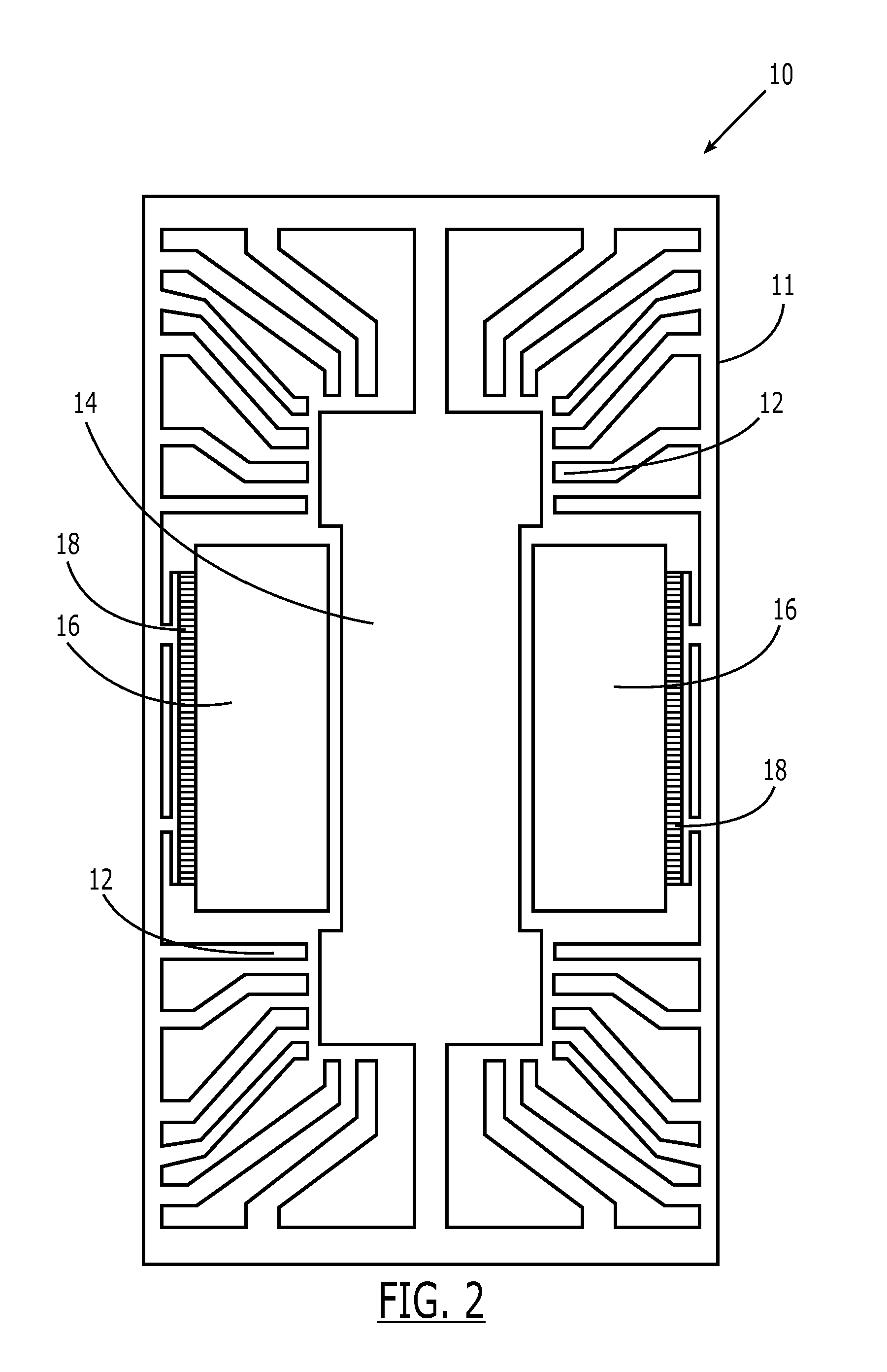
[0041]According to a first embodiment of the present invention, a template of integrated leadframe and bezel is provided for an integrated leadframe and bezel 10, as illustrated in FIG. 1. The template may, in some embodiments, represents a unit detail (the design) of a leadframe structure, in other embodiments the artwork used to pattern and etch sheet material to form a leadframe, in still other embodiments the die or other tool carrying the leadframe design used to form a leadframe, and in still further embodiments the leadframe structure itself. Thus, by definition, template as used herein is intended to cover both the design of a leadframe and the leadframe itself, as well as the tools carrying the design and used to produce the leadframe.

[0042]Integrated leadframe and bezel 10 includes a carrier frame 11. Physically and electrically connected to said carrier frame 11 are a number of bonding leads 12, a die pad region 14, and bezel regions 16, each described further below. Impo...


PUM


Abstract

An integrated leadframe and bezel structure includes a planar carrier frame, a plurality of bonding leads, a die pad region, and a bezel structure. The bezel structure includes a bending portion shaped and disposed to facilitate a portion of said bezel structure being bent out of the plane of said carrier frame. A sensor IC may be secured to the die pad region, and wire bonds made to permit external connection to the sensor IC. The bezel structure includes portions which are bent such that their upper extent is in or above a sensing surface. The assembly is encapsulated, exposing on the top surface part of the bezel portions and the upper surface of the sensor IC, and on the bottom surface the contact pads. Two or more bezel portions may be provided, one or more on each side of the sensor IC.

Description

BACKGROUND OF THE INVENTION[0001]1. Field of the Invention[0002]The present invention relates to integrated circuit packaging, and more specifically to a leadframe structure and method of using same which provides an integrated leadframe and exposed bezel portion for receiving a user's fingertip or the like.[0003]2. Description of the Prior Art[0004]The present invention lies at the crossroads of two different technologies. The first of these is integrated circuit (IC) packaging. The second is silicon fingerprint sensors. We look first at IC packaging. Historically, the number of devices formed on an IC die has increased dramatically from year to year. Advancements in both the design and layout of devices carried by the IC die as well as in designs for making external connections to those devices have supported the increases in device count. A typical IC assembly includes the die, often a body of a semiconducting material such as silicon, having interconnected electronic elements su...

Claims


Application Information

Patent Timeline
Patent Type & Authority Applications(United States)
IPC IPC(8): H01L23/495H01L21/71
CPCG06K9/00026H01L23/49551H01L2224/48091H01L2924/10253H01L2224/49171H01L2224/48247H01L2924/00014H01L2924/00G06V40/1335H01L23/49548H01L23/49541
Inventor BOND, ROBERTKRAMER, ALANGOZZINI, GIOVANNI
Owner APPLE INC
Why Eureka
Try Eureka