
Wafer singulation in high volume manufacturing

a high-volume manufacturing and wafer technology, applied in the field of semiconductor fabrication, can solve problems such as residual stress, uneven street width, rough edges,

Inactive Publication Date: 2010-05-27
INTEL CORP
View PDF18 Cites 61 Cited by
  • Summary
  • Abstract
  • Description
  • Claims
  • Application Information

AI Technical Summary

Problems solved by technology

Issues that may arise include rough edges, uneven street width, residual stress, and delamination in low-k dielectric layers on the die.

Method used


Image

  • Wafer singulation in high volume manufacturing
  • Wafer singulation in high volume manufacturing
  • Wafer singulation in high volume manufacturing

Examples


Embodiment Construction

[0011]In the following description, numerous details of specific materials, features, dimensions, processes, and sequences are set forth to provide a thorough understanding of the present invention. However, in some instances, one skilled in the art will realize that the invention may be practiced without these particular details. In other instances, one skilled in the art will also realize that certain well-known details have not been described so as to avoid obscuring the present invention.

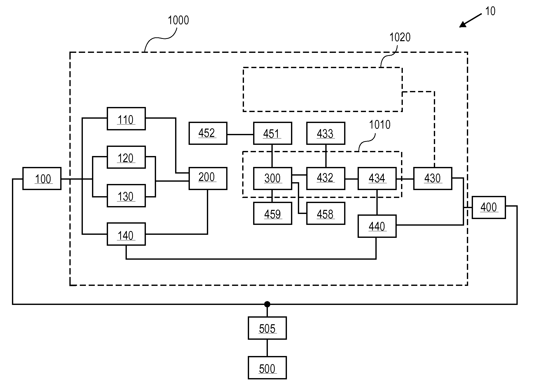
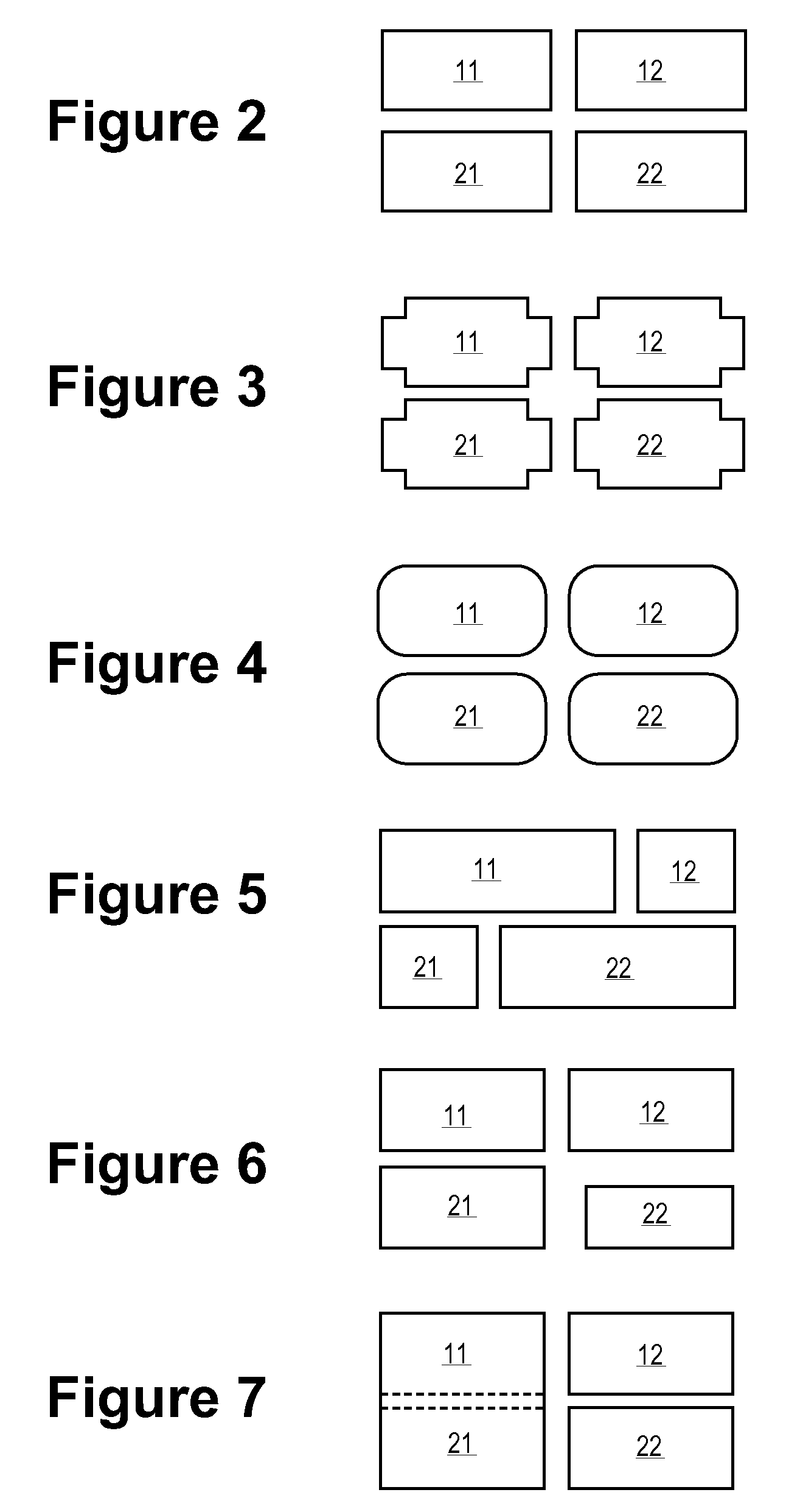
[0012]An apparatus 10 (as shown in FIG. 1) for, a method (as shown in FIGS. 8-9) of, and the resultant structures (as shown in FIGS. 2-7) formed by laser scribing and laser-assisted chemical singulation, such as along scribelines or streets of a substrate, and such as in high volume manufacturing (HVM), according to various embodiments of the present invention will be described below.

[0013]In an embodiment of the present invention as shown in FIG. 1, the substrate 300 includes a whole wafer. In ...


PUM

PropertyMeasurementUnit
thicknessaaaaaaaaaa
diameteraaaaaaaaaa
thicknessaaaaaaaaaa

Abstract

The present invention discloses an apparatus including: a laser beam directed at a wafer held by a chuck in a process chamber; a focusing mechanism for the laser beam; a steering mechanism for the laser beam; an optical scanning mechanism for the laser beam; a mechanical scanning system for the chuck; an etch chemical induced by the laser beam to etch the wafer and form volatile byproducts; a gas feed line to dispense the etch chemical towards the wafer; and a gas exhaust line to remove any excess of the etch chemical and the volatile byproducts.

Description

CROSS REFERENCE TO RELATED APPLICATION[0001]This is a Continuation-in-part of serial No. (TBD), filed on Oct. 28, 2008, which is currently pending.BACKGROUND OF THE INVENTION[0002]1. Field of the Invention[0003]The present invention relates to a field of semiconductor fabrication and, more specifically, to an apparatus for and method of singulating a wafer in high volume manufacturing.[0004]2. Discussion of Related Art[0005]Singulating a wafer involves separation of a substrate into individual die. A backside of a wafer to be singulated is first subjected to backgrinding, followed by polishing. Then, a laser beam is used from the backside of the wafer to form a series of modified layers inside the wafer, extending from the active surface of the wafer to the backside of the wafer. Deterioration sites are formed in the modified layers along scribelines that are arranged in a lattice pattern across an active surface of the wafer. Then, the wafer is mounted onto a dicing tape and singul...

Claims


Application Information

Patent Timeline
Patent Type & Authority Applications(United States)
IPC IPC(8): H01L21/02B23K26/02
CPCB23K26/0635B23K26/0736B23K26/0807B23K26/0853B23K26/12B23K26/127B23K26/4075B23K2201/40H01L21/3065H01L21/67092H01L21/78B23K26/367B23K26/364B23K26/082B23K26/0624B23K26/40B23K2101/40B23K2103/50
Inventor VAKANAS, GEORGECHEN, GEORGEGREENZWEIG, YUVALLI, ERICVORONOV, SERGEI
Owner INTEL CORP
Features
  • Generate Ideas
  • Intellectual Property
  • Life Sciences
  • Materials
  • Tech Scout
  • Unparalleled Data Quality
  • Higher Quality Content
  • 60% Fewer Hallucinations
Learn More