Semiconductor device having active element connected to an electrode metal pad via a barrier metal layer and interlayer insulating film

a technology of active elements and semiconductor devices, applied in the direction of semiconductor devices, semiconductor/solid-state device details, electrical apparatus, etc., to achieve the effect of avoiding the exfoliation of the pad

Inactive Publication Date: 2005-03-08
SHARP KK
View PDF14 Cites 63 Cited by
  • Summary
  • Abstract
  • Description
  • Claims
  • Application Information

AI Technical Summary

Benefits of technology

The object of the present invention is to provide a semiconductor device of an area pad ...

Problems solved by technology

As a result, the semiconductor device of the area pad structure wherein the electrode pad is formed on the active elemen...

Method used


Image

  • Semiconductor device having active element connected to an electrode metal pad via a barrier metal layer and interlayer insulating film
  • Semiconductor device having active element connected to an electrode metal pad via a barrier metal layer and interlayer insulating film
  • Semiconductor device having active element connected to an electrode metal pad via a barrier metal layer and interlayer insulating film

Examples


second embodiment

The following description will explain another embodiment of the present invention, while referring to the drawings. The members having the same structure (function) as those in the above-mentioned embodiment will be designated by the same reference numerals and their description will be omitted.

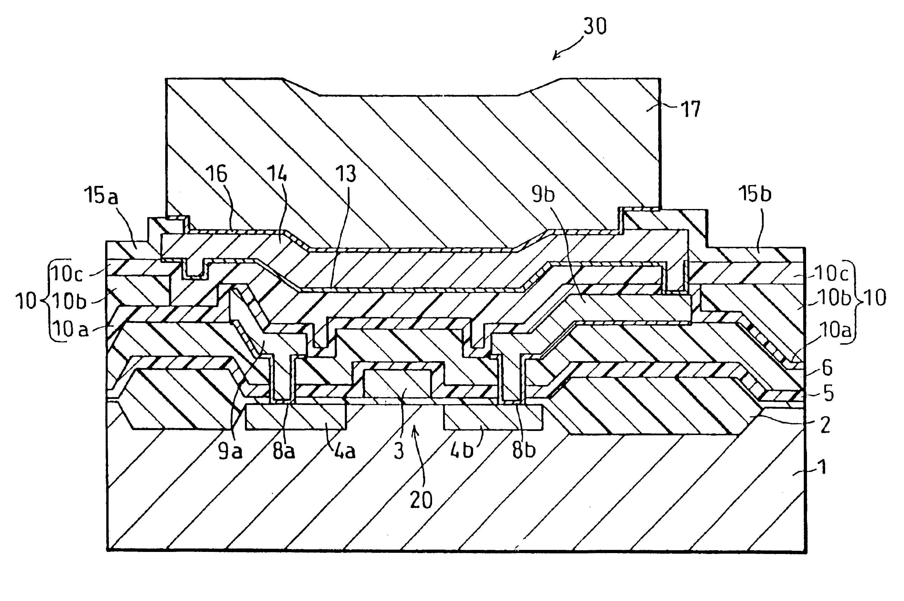
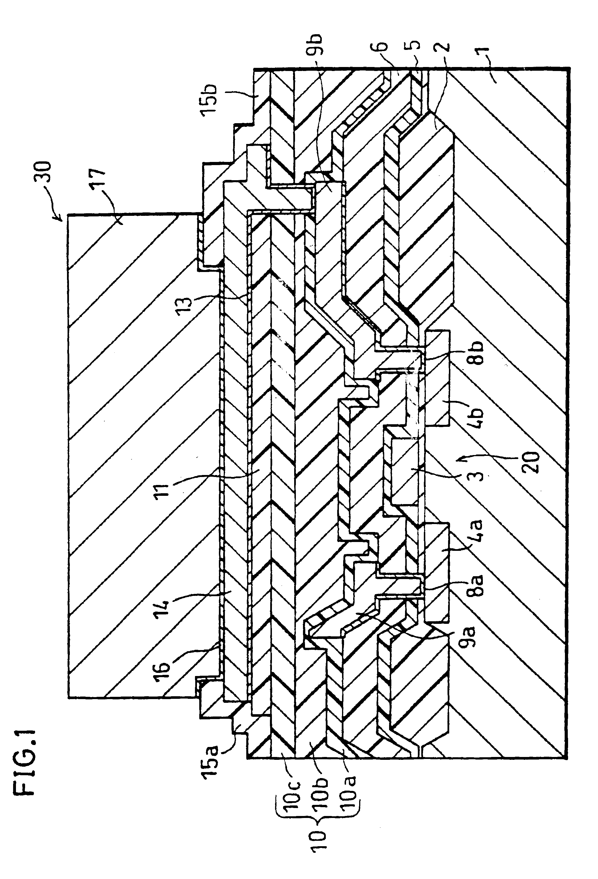
As shown in FIG. 5, a semiconductor chip in accordance with the present embodiment has the same arrangement as that of the semiconductor chip shown in FIG. 1 except that: (1) the insulating film 11 is not formed on the third interlayer insulating film 10c; and (2) a portion of the second interlayer insulating film 10b right under the second metal layer 14 is removed.

A manufacturing process of a semiconductor device arranged as above is as follows. The manufacture proceeds through the same steps as those in the first embodiment till the step shown in FIG. 4(c), and then, a film containing silicon, that is, either a silicon oxide film, a silicon nitride film, or a film made of TEOS is formed a...

third embodiment

The following description will explain still another embodiment of the present invention, while referring to the drawings. The members having the same structure (function) as those in the above-mentioned embodiment will be designated by the same reference numerals and their description will be omitted.

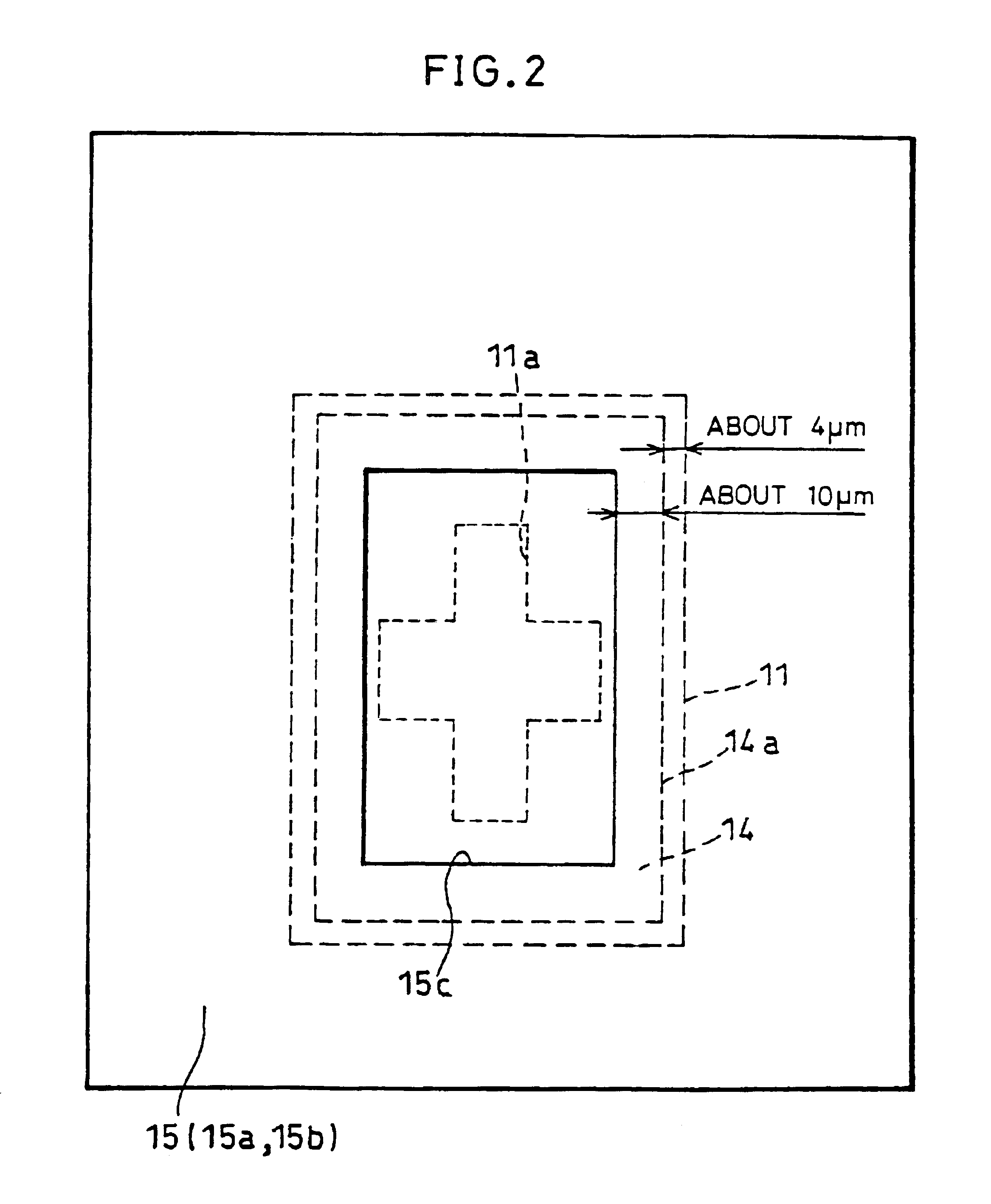
As shown in FIG. 8, the passivation film 15 (15a and 15b), which is normally formed so as to cover a part of the second metal layer 14, is formed, in the present embodiment, so as to cover a greater part of the second metal layer 14, so that the stress occurring upon bonding or after bonding is eased. The rest of the arrangement is the same as that in the first embodiment except that the insulating film 11 is provided in the first embodiment while it is not in the present embodiment.

In this case, as shown in FIG. 9, since the second metal layer 14 is 50 μm×100 μm in size, the passivation film 15 (15a and 15b) is formed so as to cover a large part of the second metal layer 14, with an o...

fourth embodiment

The following description will explain another embodiment of the present invention, while referring to the drawings. The members having the same structure (function) as those in the first through third embodiments will be designated by the same reference numerals and their description will be omitted.

As shown in FIG. 10, in the present embodiment, an interlayer insulating film 40 having a quintuple layer structure (hereinafter referred to as a quintuple-structure interlayer insulating film 40) is formed between the second metal layer 14 and the first metal layers 9a and 9b, so that high reliability is obtained in environmental tests during or after an inner lead bonding (ILB) operation. The arrangement of the present embodiment is completely identical to that of the first embodiment except that the above interlayer insulating film 40 is provided.

A first layer (a first-layer insulating film 40a) of the foregoing interlayer insulating film having the quintuple layer structure (hereina...


PUM


Abstract

A semiconductor device of the present invention has (1) an active element provided on a semiconductor substrate, (2) an interlayer insulating film formed so as to cover the active element, (3) a pad metal for an electrode pad which is provided on the interlayer insulating film, (4) a barrier metal layer which is provided on the active element with the interlayer insulating film therebetween, so that the pad metal is formed on the barrier metal layer, and (5) an insulating layer having high adherence to the barrier metal layer, the insulating layer being provided between the interlayer insulating film and the barrier metal layer. With this arrangement, the adherence between the barrier metal layer, the insulating film and the interlayer insulating film is surely improved, and even in the case where an external force is applied to the electrode pad upon bonding or after bonding, the barrier metal layer hardly comes off the part thereunder. Therefore, the breakdown of a level difference compensating film, and the exfoliation of the barrier metal layer from the interlayer insulating film can be prevented, while the semiconductor device of the area pad structure featuring lower costs, high quality, and high liability is constantly mass-produced. Besides, the yield of the semiconductor device is surely improved.

Description

FIELD OF THE INVENTIONThe present invention relates to a semiconductor integrated circuit device (hereinafter simply referred to as semiconductor device) for use in, for example, a liquid crystal driver or the like, and more particularly, relates to an electrode pad structure of a semiconductor device.BACKGROUND OF THE INVENTIONConventionally, semiconductor chips (semiconductor devices) featuring a double metal structure have been mass-produced, and most of the semiconductor chips of this type are arranged so that each includes an electrode pad 70 in an area other than a circuit element area therein, as shown in FIG. 19.More specifically, for example, a silicon oxide film (hereinafter referred to as CVD-silicon oxide film) 55 formed by the low-pressure chemical vapor deposition (CVD) method and a boron phospho-silicate glass (BPSG) film 56 are laminated on a silicon substrate 51 in this order. On the BPSG film 56, a barrier metal layer 58 and a first metal layer 59 are provided in t...

Claims


Application Information

Patent Timeline
IPC IPC(8): H01L23/52H01L23/485H01L23/532H01L23/48H01L21/60H01L21/316H01L21/3205
CPCH01L23/5329H01L24/10H01L24/13H01L2224/4847H01L2924/35121H01L2924/00014H01L2924/01033H01L24/45H01L2224/13099H01L2224/45124H01L2224/45144H01L2924/01005H01L2924/01013H01L2924/01014H01L2924/01022H01L2924/01029H01L2924/01074H01L2924/01075H01L2924/01078H01L2924/01079H01L2924/01082H01L2924/14H01L2924/01006H01L2924/00H01L24/05H01L24/48H01L2224/0401H01L2224/04042H01L2224/05556H01L2224/05558H01L2224/05572H01L2224/05624H01L2224/10H01L2224/13H01L2224/13144H01L2224/14104H01L2224/48624H01L2224/48724H01L2924/01015H01L2924/351H01L2924/00012H01L21/32H01L2224/45
Inventor TOYOSAWA, KENJIONO, ATSUSHICHIKAWA, YASUNORISAKAGUCHI, NOBUHISANAKAMURA, NAKAENAKATA, YUKINORI
Owner SHARP KK
Why Eureka
Try Eureka