Eureka AIR delivers breakthrough ideas for toughest innovation challenges, trusted by R&D personnel around the world.

Apparatus and method for washing polycrystalline silicon

Active Publication Date: 2010-06-03
MITSUBISHI MATERIALS CORP
View PDF8 Cites 9 Cited by
  • Summary
  • Abstract
  • Description
  • Claims
  • Application Information

AI Technical Summary

Benefits of technology

[0010]The present invention has been made in order to solve the above-mentioned problems, and an object of the present invention is to provide a washing apparatus and a washing method capable of obtaining high-quality polycrystalline silicon having reduced impurities or spots.
[0017]In two or more adjacent acid baths, the concentration of impurities in the first acid bath, is the highest. On the other hand, the concentration of impurities in the last acid bath is the lowest. That is, the concentration of impurities is gradually lowered from the former acid bath to the later acid bath between the first acid bath and the last acid bath. Therefore, the acid including a low concentration of impurities is reused as a washing liquid of the former acid bath including the acid with an impurity concentration higher than that of the later acid bath. As a result, it is possible to use expensive chemicals effectively.
[0019]The polycrystalline silicon washing apparatus according to the present invention may further include at least one intermediate pure water bath which is provided between the first acid bath and the last acid bath and is filled with pure water and into which the polycrystalline silicon is immersed. According to the above-mentioned structure, even when impurities in the acid bath re-adhere to the polycrystalline silicon after the polycrystalline silicon is immersed into the acid bath before the intermediate pure water bath to be washed and is then brought out from the acid bath, it is possible to wash the impurities in the intermediate pure water bath. Therefore, it is possible to prevent the impurities re-adhered to the polycrystalline silicon in the former acid bath from being carried into the later acid bath into which the polycrystalline silicon is immersed after the intermediate pure water bath.
[0022]According to the present invention, in the first acid bath, the polycrystalline silicon actively reacts with the acid to remove impurities, and the spots generated in the first acid bath are removed by the later acid bath with a lower temperature. Therefore, it is possible to effectively remove impurities from the surface of the polycrystalline silicon and obtain high-quality polycrystalline silicon having reduced any spots. It is possible to reduce the influence of a variation in the reaction of the polycrystalline silicon immersed into each acid bath and perform a stable reaction by providing a temperature adjusting unit in each acid bath.
[0023]In addition, it is possible to reuse the acid used in the later acid bath as a washing liquid of the former acid bath, by moving a portion of the acid in the later acid bath to the former acid bath. In this way, it is possible to reduce the amount of acid used. Further, since the above-mentioned processes are continuously performed without being stopped, it is possible to obtain high productivity.

Problems solved by technology

However, when the temperature of the acid is increased in order to accelerate the reaction, the surface of the polycrystalline silicon is rapidly oxidized or dissolved by the chemicals used.

Method used


Image

  • Apparatus and method for washing polycrystalline silicon
  • Apparatus and method for washing polycrystalline silicon
  • Apparatus and method for washing polycrystalline silicon

Examples


Embodiment Construction

[0028]Hereinafter a polycrystalline silicon washing apparatus according to an embodiment of the present invention will be described with reference to the accompanying drawings.

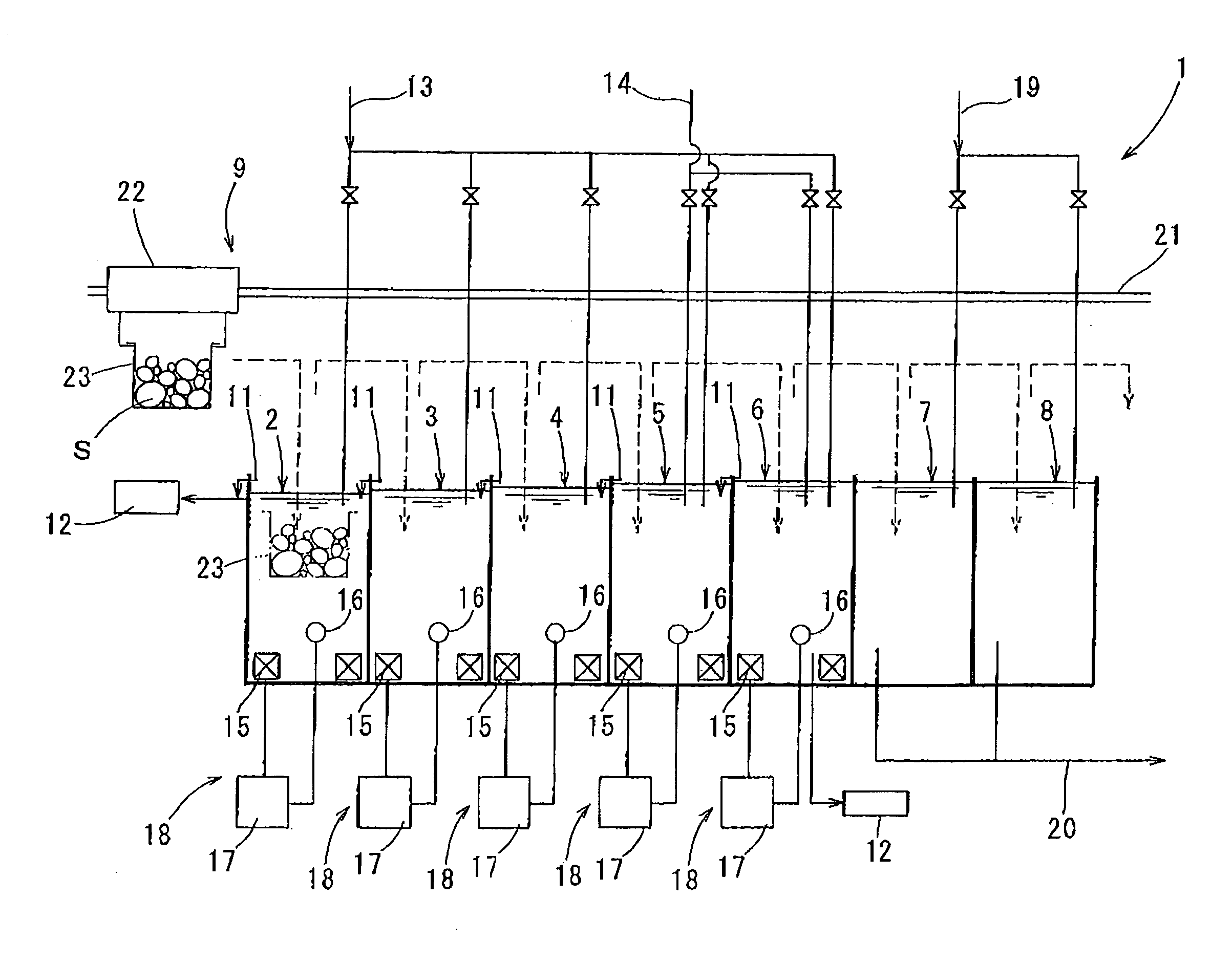
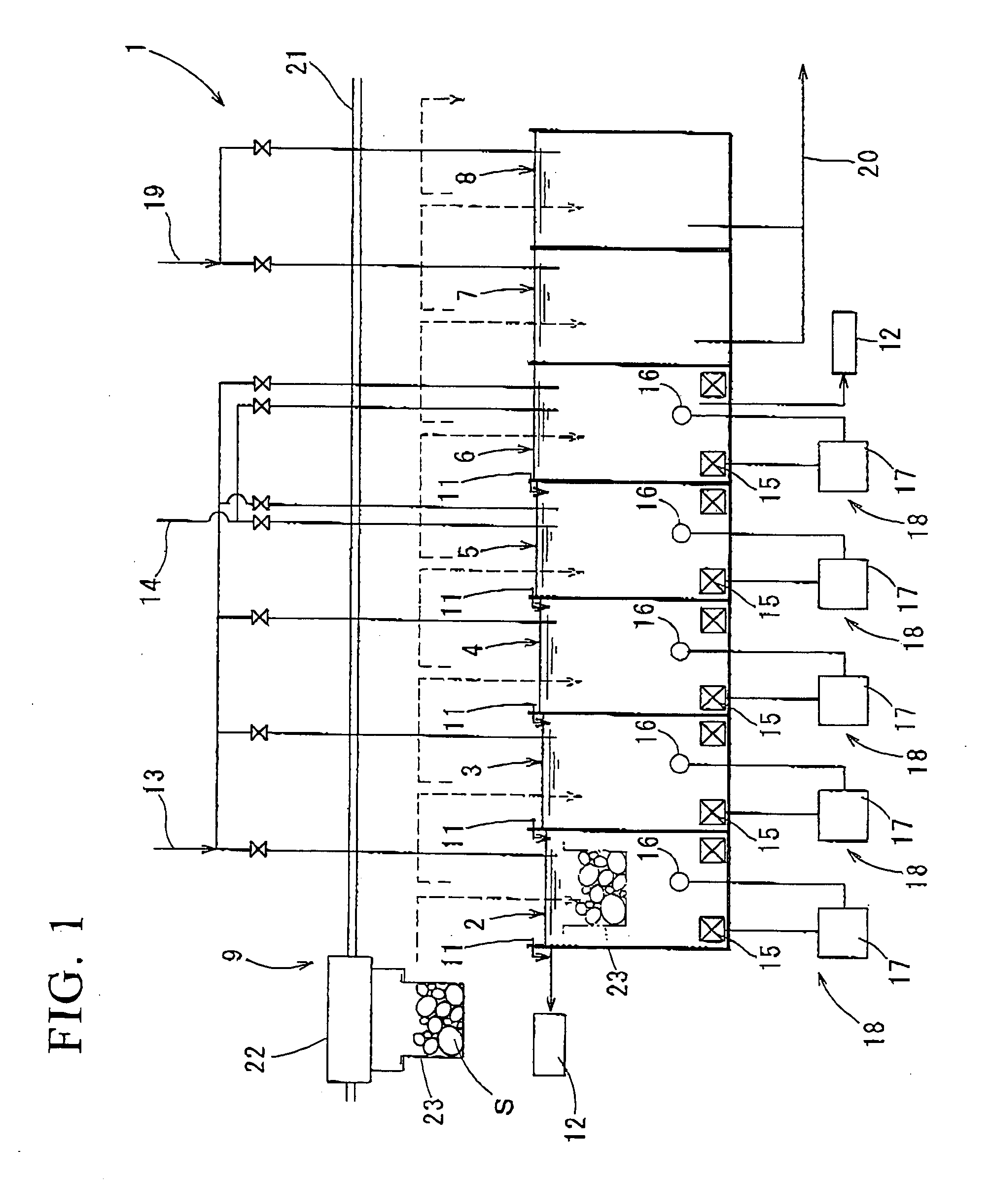
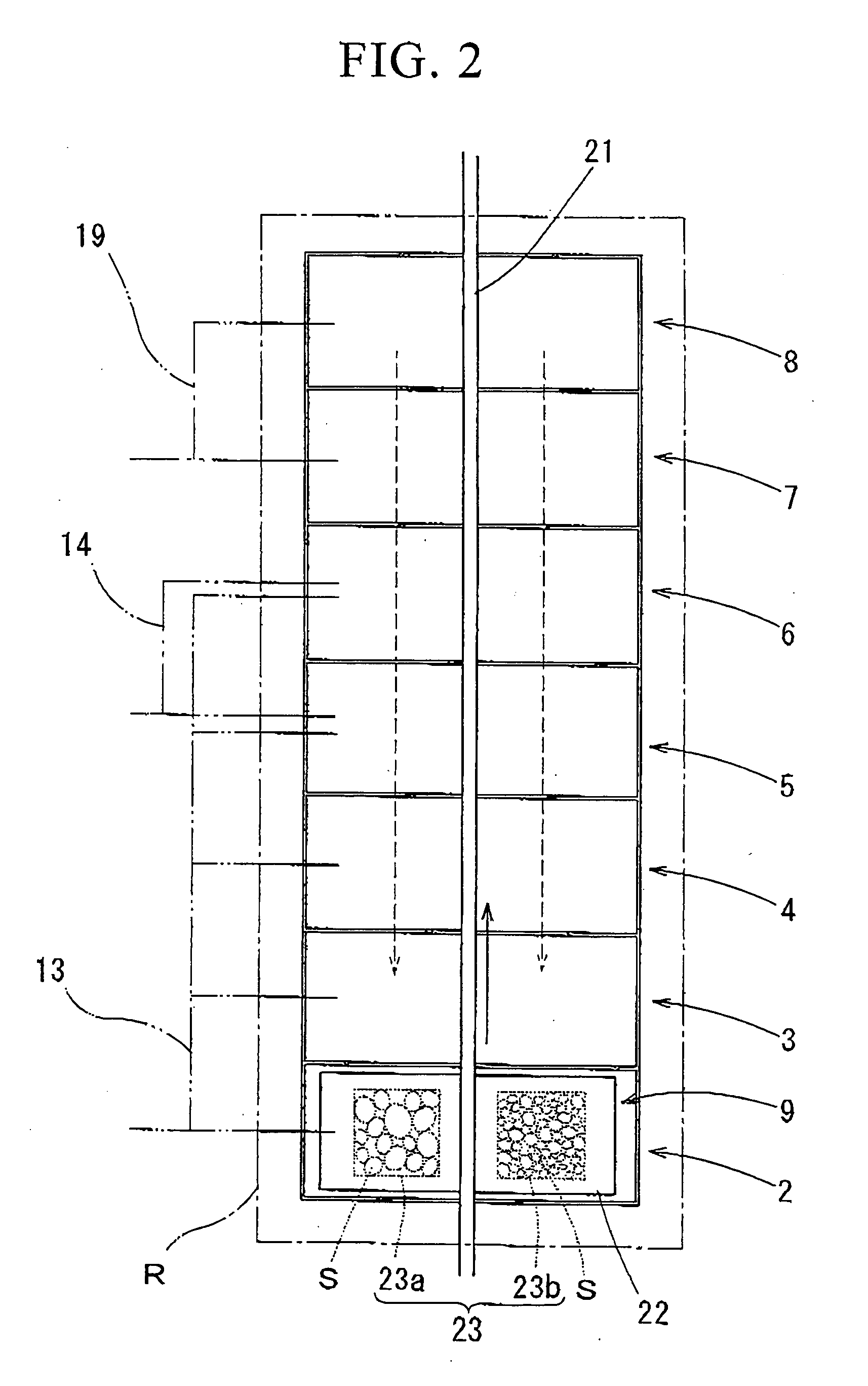
[0029]FIGS. 1 and 2 show a first embodiment. A washing apparatus 1 according to the first embodiment includes five acid baths 2 to 6 each filled with an acid and two pure water baths 7 and 8 each filled with pure water, which are arranged in a straight line (hereinafter, the acid baths and the pure water baths are collectively referred to as ‘baths’). A transporting unit 9 that sequentially transports a polycrystalline silicon S to the baths 2 to 8 is provided above the baths. The acid baths 2 to 6 are referred to as the first bath 2 to fifth bath 6 in the order in which the polycrystalline silicon is immersed. The size of the each bath is, for example, 600 mm (L)×1200 mm (W)×630 mm (D).

[0030]In each of the acid baths 2 to 6, a mixed solution of a hydrofluoric acid and a nitric acid is used as the acid. In thi...


PUM


Abstract

Disclosed is a polycrystalline silicon washing apparatus that sequentially immerses polycrystalline silicon into a plurality of acid baths each of which is filled with an acid to wash the polycrystalline silicon. The temperatures of the acids in the acid baths are set such that the temperature of the acid in a later acid bath of adjacent acid baths is equal to or lower than that of a former acid bath and the temperature of the acid in the last acid bath is lower than that of the acid in the first acid bath. Each of the acid baths is provided with a temperature adjusting unit that controls the temperature of the acid at a constant value.

Description

BACKGROUND OF THE INVENTION[0001]1. Field of the Invention[0002]The present invention relates to an apparatus and method for washing lump or rod-shaped polycrystalline silicon, which is a raw material of single crystal silicon for semiconductors and silicon for solar cells.[0003]Priority is claimed on Japanese Patent Application No. 2008-303822, filed Nov. 28, 2008, the content of which is incorporated herein by reference.[0004]2. Description of Related Art[0005]In general, single crystal silicon used for semiconductor devices is produced by a Czochralski method. In the Czochralski method, lump or rod-shaped polycrystalline silicon or single crystal silicon is melted in a quartz crucible, a seed crystal is dipped into the obtained melt, and the seed crystal is pulled to grow a single crystal silicon. In order to obtain high-quality single crystal silicon, it is necessary to minimize the amount of impurities adhered to the surface of the lump or rod-shaped polycrystalline silicon.[00...

Claims


Application Information

Patent Timeline
IPC IPC(8): B08B3/08B08B13/00
CPCC01B33/037
Inventor SAKAI, KAZUHIROATSUMI, TETSUYAMIYATA, YUKIYASU
Owner MITSUBISHI MATERIALS CORP
Why Eureka
Eureka Blog
Learn More