Film deposition apparatus, film deposition method, semiconductor device fabrication apparatus, susceptor for use in the same, and computer readable storage medium

US20100136795A1Inactive Publication Date: 2010-06-03TOKYO ELECTRON LTD

Image

  • Film deposition apparatus, film deposition method, semiconductor device fabrication apparatus, susceptor for use in the same, and computer readable storage medium
  • Film deposition apparatus, film deposition method, semiconductor device fabrication apparatus, susceptor for use in the same, and computer readable storage medium
  • Film deposition apparatus, film deposition method, semiconductor device fabrication apparatus, susceptor for use in the same, and computer readable storage medium

Examples


Embodiment Construction

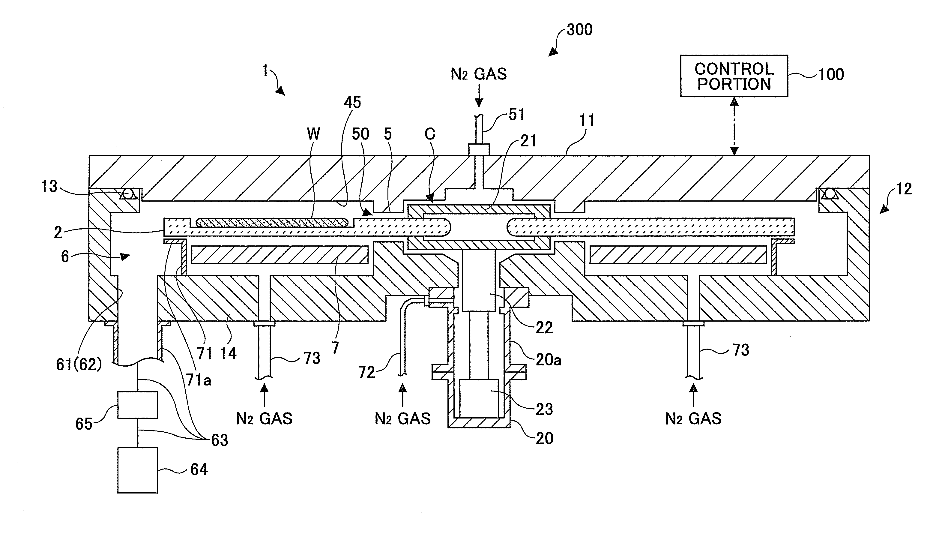
[0042]According to an embodiment of the present invention, there are provided a film deposition apparatus, a film deposition method, a semiconductor device fabrication apparatus, and a susceptor to be used for the apparatuses that are capable of preventing a problem caused when a substrate is placed by lift pins, and a computer readable storage medium that stores a computer program that causes the film deposition apparatus to perform the film deposition method.

[0043]Referring to the accompanying drawings, a film deposition film according to an embodiment of the present invention is explained in the following.

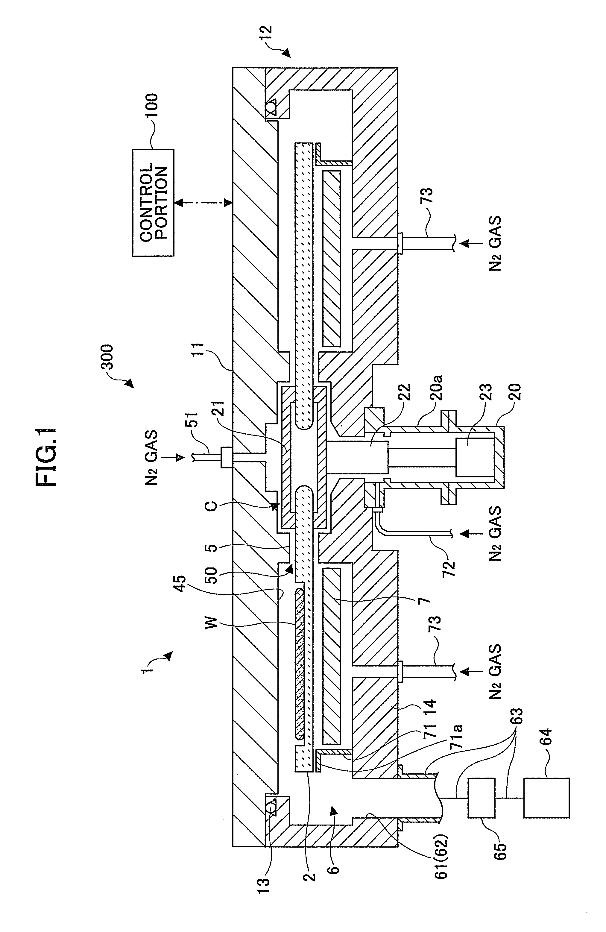
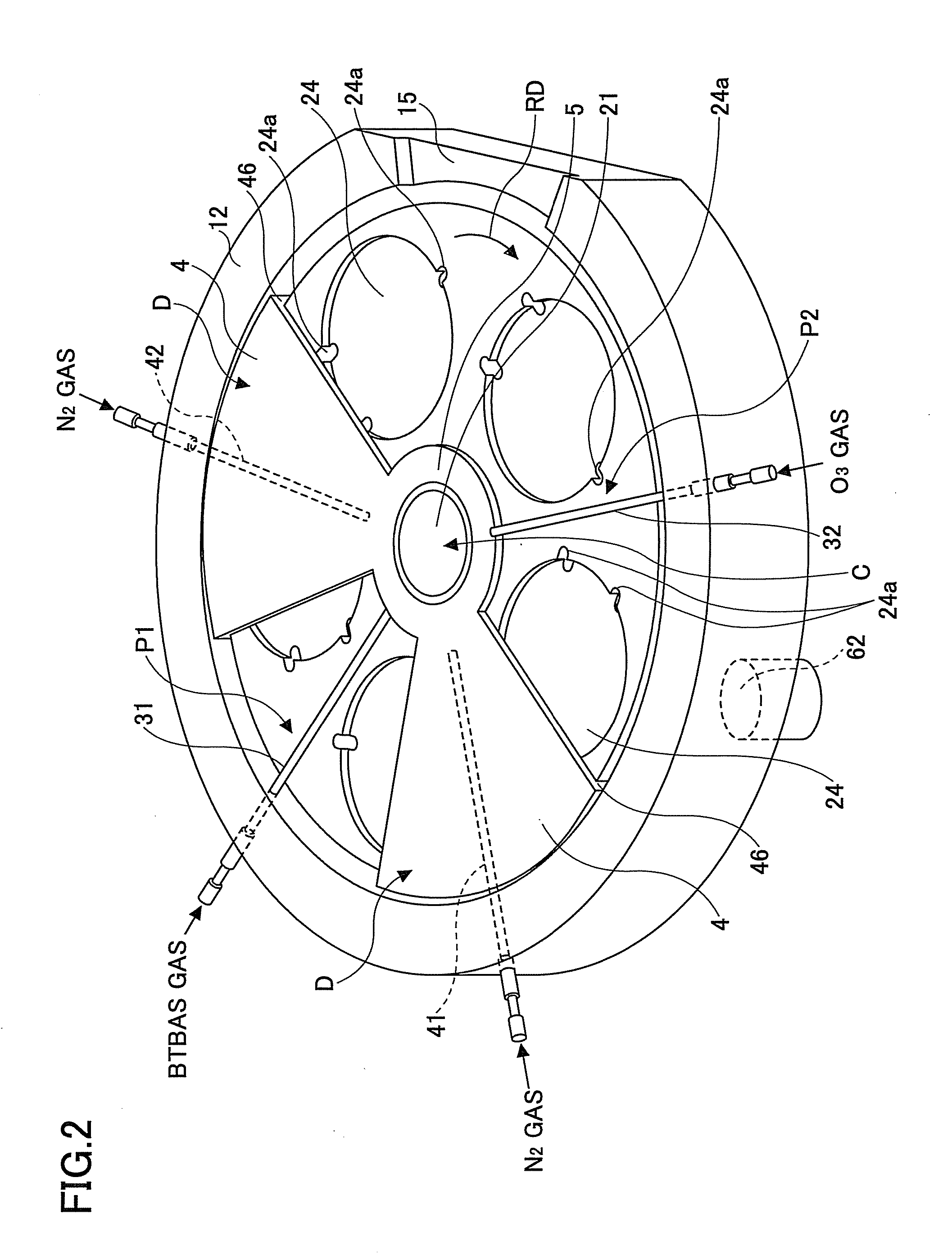
[0044]Referring to FIG. 1, which is a cross-sectional view taken along B-B line in FIG. 3, a film deposition apparatus 300 according to this embodiment of the present invention has a vacuum chamber 1 having a flattened cylinder shape, and a susceptor 2 that is located inside the vacuum chamber 1 and has a rotation center at a center of the vacuum chamber 1. The vacuum chamber 1 ...


PUM

PropertyMeasurementUnit
Areaaaaaaaaaaa

Abstract

A disclosed semiconductor device fabrication apparatus includes a chamber where a predetermined process is carried out with respect to a substrate; a transfer arm that includes claw portions for supporting a lower peripheral surface portion of the substrate and that moves into and out from the chamber; and a susceptor that includes a substrate receiving portion in which the substrate is placed, and a step portion provided to allow the claw portions to move to a position lower than an upper surface of the substrate receiving portion.

Description

CROSS-REFERENCE TO RELATED APPLICATION[0001]This application claims the benefit of priority of Japanese Patent Application No. 2008-305341, filed on Nov. 28, 2008, with the Japanese Patent Office, the entire contents of which are hereby incorporated by reference.BACKGROUND OF THE INVENTION[0002]1. Field of the Invention[0003]The present invention relates to a film deposition apparatus, a film deposition method, a semiconductor device fabrication apparatus, a susceptor for use in the same, and a computer readable storage medium.[0004]2. Description of the Related Art[0005]In order to fabricate semiconductor devices, semiconductor device fabrication apparatuses including a film deposition apparatus, an etching apparatus, a thermal processing apparatus and the like are used. In these semiconductor device fabrication apparatuses, a semiconductor substrate (wafer) is placed in a susceptor provided in accordance with a type of the semiconductor device fabrication apparatus. For example, s...

Claims


Application Information

Patent Timeline
03 Jun 2010
Publication
US20100136795A1
IPC
H01L21/30; C23C16/458
CPC
C23C16/45551; H01L21/31608; H01L21/67748; H01L21/68792; H01L21/68742; H01L21/68764; H01L21/68771; H01L21/68707
Inventors
HONMA, MANABU