Display apparatus

a display apparatus and contact hole technology, applied in the direction of discharge tube/lamp details, discharge tube luminescnet screens, organic semiconductor devices, etc., can solve the problems of unnecessarily increasing opening area, power loss, difficulty in achieving narrow frames, etc., to achieve the effect of reducing power loss and without increasing parasitic resistan

Active Publication Date: 2010-06-10
CANON KK
View PDF4 Cites 7 Cited by
  • Summary
  • Abstract
  • Description
  • Claims
  • Application Information

AI Technical Summary

Benefits of technology

[0012]The present invention has been achieved to decrease power losses and achieve a narrow frame without increasing a parasitic resistance reducing currents intensively flowing into contact holes.

Problems solved by technology

Further, currents intensively flow into the contact holes and the parasitic resistances are increased in appearance, which may cause power losses.
The above-described problem occurs especially when a TCO electrode with a high resistance is electrically connected to wiring with a resistance lower than the resistance of the TCO electrode.
Consequently, the opening area is unnecessarily increased in relation to the amount of currents flowing into the contact holes provided at a distance from the display region so that a narrow frame may be achieved with difficulty.

Method used


Image

  • Display apparatus
  • Display apparatus
  • Display apparatus

Examples


first embodiment

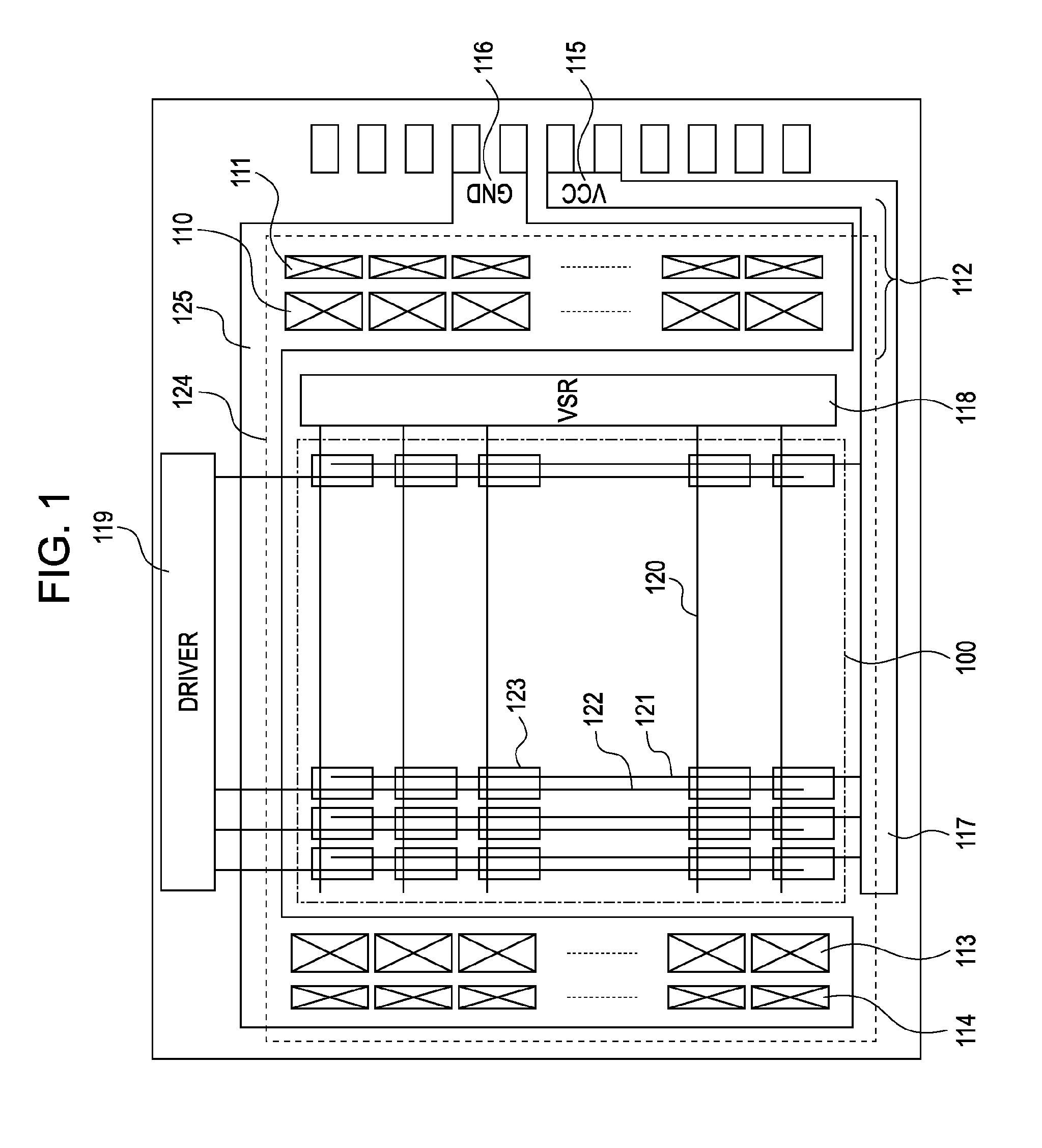
[0021]The configuration of a display panel will now be described in accordance with the present invention with reference to FIG. 1. First, a thin film transistor (TFT) and a planarization film are provided on a substrate. Then, a transparent conductive oxide (TCO) electrode 124 (first electrode including an indium tin oxide (ITO), etc.) provided on the light extraction side and a second electrode (including aluminum (Al), for example) are provided on the planarization film to sandwich a light emitting layer (not shown) between the TCO electrode 124 and the second electrode. The light emitting layer may be, for example, an organic film which emits light when an electrical potential is applied across the film.

[0022]Next, a contact hole 1 (110 and 113) and a contact hole 2 (111 and 114) are provided in a current path extending from the TCO electrode 124 to a ground (GND) end 116 and a PAD section 148 (shown in FIG. 3).

[0023]First, a current flowing from the TCO electrode 124 (first ele...

second embodiment

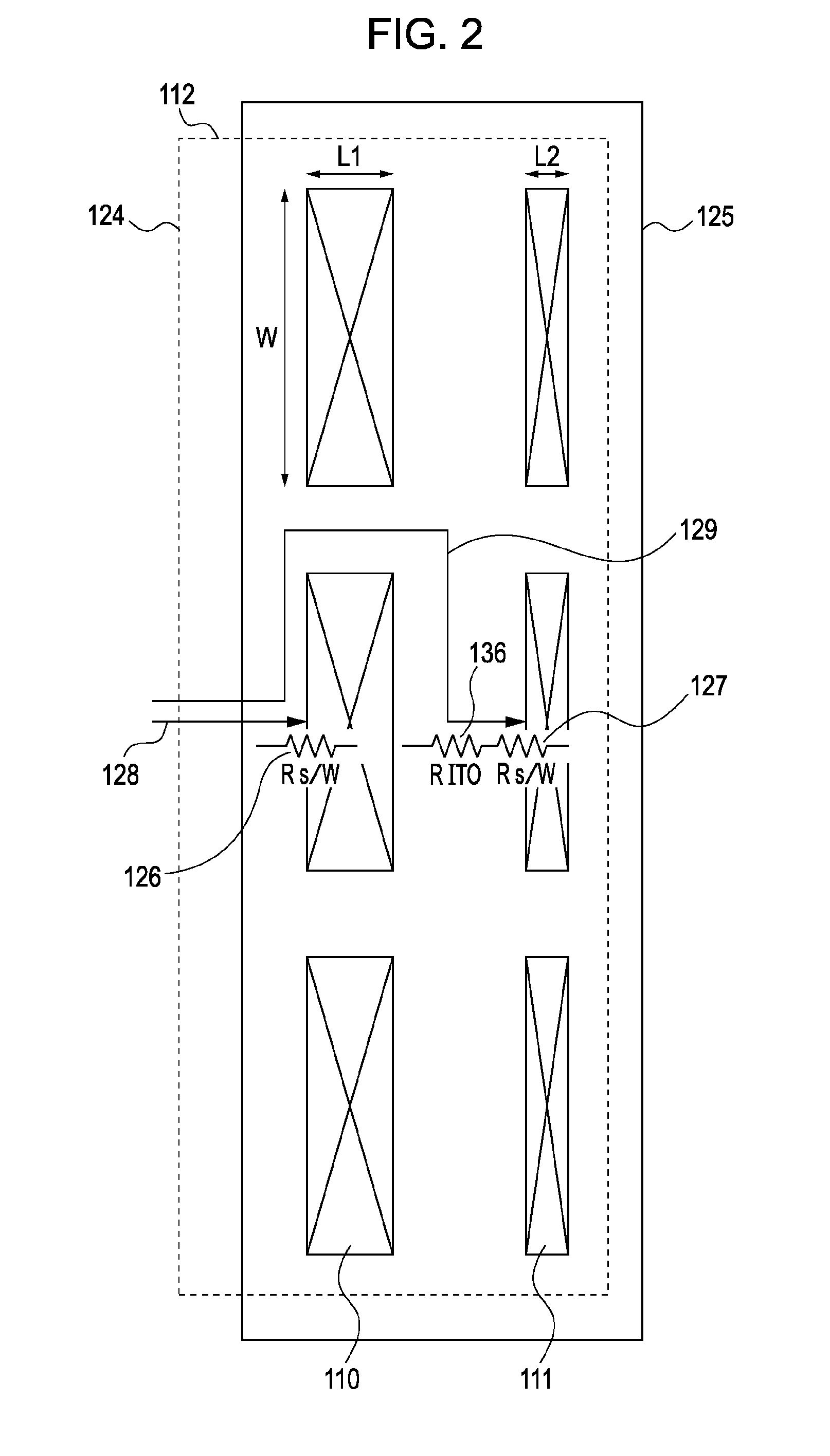
[0033]In FIG. 2, the vertical length and the horizontal length of the contact hole 1 (110 and 113) are determined to be W and L1. Further, the vertical length and the horizontal length of the contact hole 2 (111 and 114) are determined to be W and L2. In the above-described embodiment, the contact holes 1 and 2 are arranged in the form of grating. In the present invention, which will be described later, the contact holes 1 and 2 are staggered.

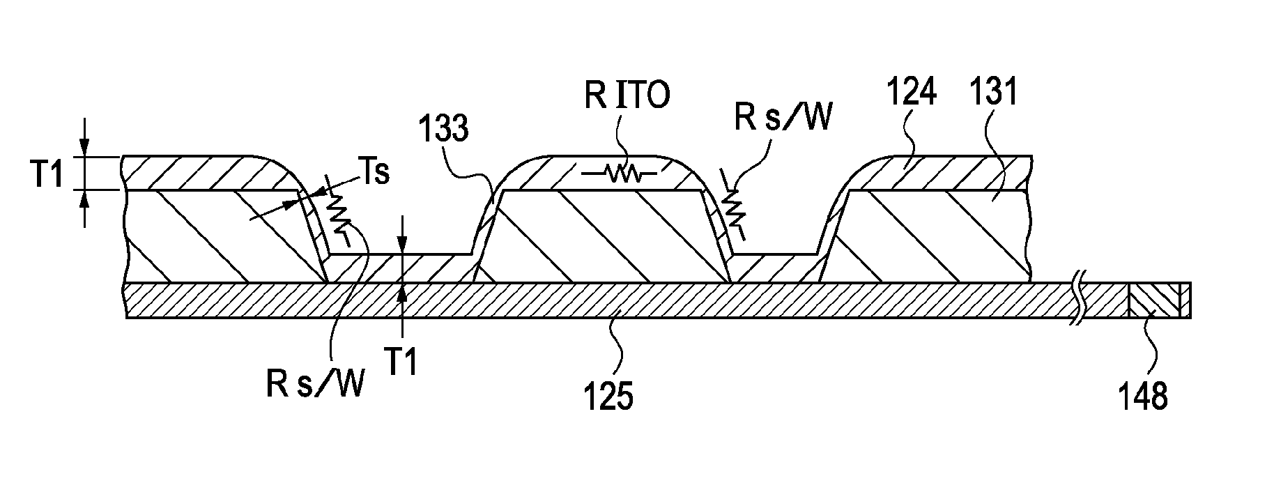
[0034]Further, in FIG. 3 which will be described below, the opening size of the contact hole at the bottom thereof is different from that of the contact hole at the uppermost part of the side wall thereof.

[0035]The inclination width is negligibly small compared with the opening size, and the opening size observed at the bottom is almost equal to that observed at the uppermost part of the side wall. Therefore, the horizontal length is determined to be L1 and / or L2.

[0036]In FIG. 2, each of current paths 128 and 129 that are provided for currents ...


PUM


Abstract

In a display apparatus, a thin film transistor, a planarization film, and at least two light-emitting devices are provided on a substrate, and the light-emitting device at least includes a light-emitting layer and first and second electrodes. At least two first contact holes and at least two second contact holes are provided in the planarization film at a part outside a display region and connect the first electrode to ground wiring and / or power wiring with a resistance lower than that of the first electrode, the distance between the second contact hole and the display region is longer than that between the first contact hole and the display region, and the opening area of the second contact hole is smaller than that of the first contact hole.

Description

BACKGROUND OF THE INVENTION[0001]1. Field of the Invention[0002]The present invention relates to the shape of a contact hole provided in a display apparatus, the shape being determined when a transparent conductive oxide (TCO) electrode is connected to wiring (power wiring and / or ground (GND) wiring).[0003]2. Description of the Related Art[0004]A light-emitting device using organic electro luminescence (hereinafter referred to as organic EL) has been provided, for example, for a matrix display apparatus that can perform full-color light emission, the matrix display apparatus including a pixel with a film provided on a substrate, where the film includes materials producing colors including red (R), green (G), and blue (B).[0005]Here, as a method of moving an upper electrode provided on the light-extraction side from a high sheet resistance such as an indium tin oxide (ITO) to GND wiring with a low sheet resistance including aluminum (Al), the method being performed in the light-emitt...

Claims


Application Information

Patent Timeline
Patent Type & Authority Applications(United States)
IPC IPC(8): H01J1/62
CPCH01L2251/5315H01L27/3276H10K59/131H10K2102/3026
Inventor MARU, HIROYUKI
Owner CANON KK
Why Eureka
Try Eureka