Semiconductor memory device and driving method thereof

Inactive Publication Date: 2010-06-10
SK HYNIX INC
View PDF2 Cites 7 Cited by
  • Summary
  • Abstract
  • Description
  • Claims
  • Application Information

AI Technical Summary

Benefits of technology

[0027]The present invention can guarantee an enough data transfer time for transferring data from a bit line pair to a segment input / output line pair in a semiconductor memory device having a low voltage level of an external supply voltage by controlling a pulse width of a column selection signal according to a voltage level of the external supply voltage. Also, the present invention may provide minimum power consumption and effective circuit operation in a semiconductor memory device having a high voltage level of an external supply voltage.

Problems solved by technology

It may cause following two problems.
It means that data is not accurately transferred to the bit line pair BL and / BL.
However, a semiconductor memory device may consume electric power unnecessarily because the time of connecting the bit line pair BL and / BL with the segment input / output line pair SIO and / SIO is unnecessary long.
Furthermore, circuit operation efficiency may be deteriorated because the column selection signal YI is activated for unnecessarily long time.

Method used


Image

  • Semiconductor memory device and driving method thereof
  • Semiconductor memory device and driving method thereof
  • Semiconductor memory device and driving method thereof

Examples


Embodiment Construction

[0035]Other objects and advantages of the present invention can be understood by the following description, and become apparent with reference to the embodiments of the present invention.

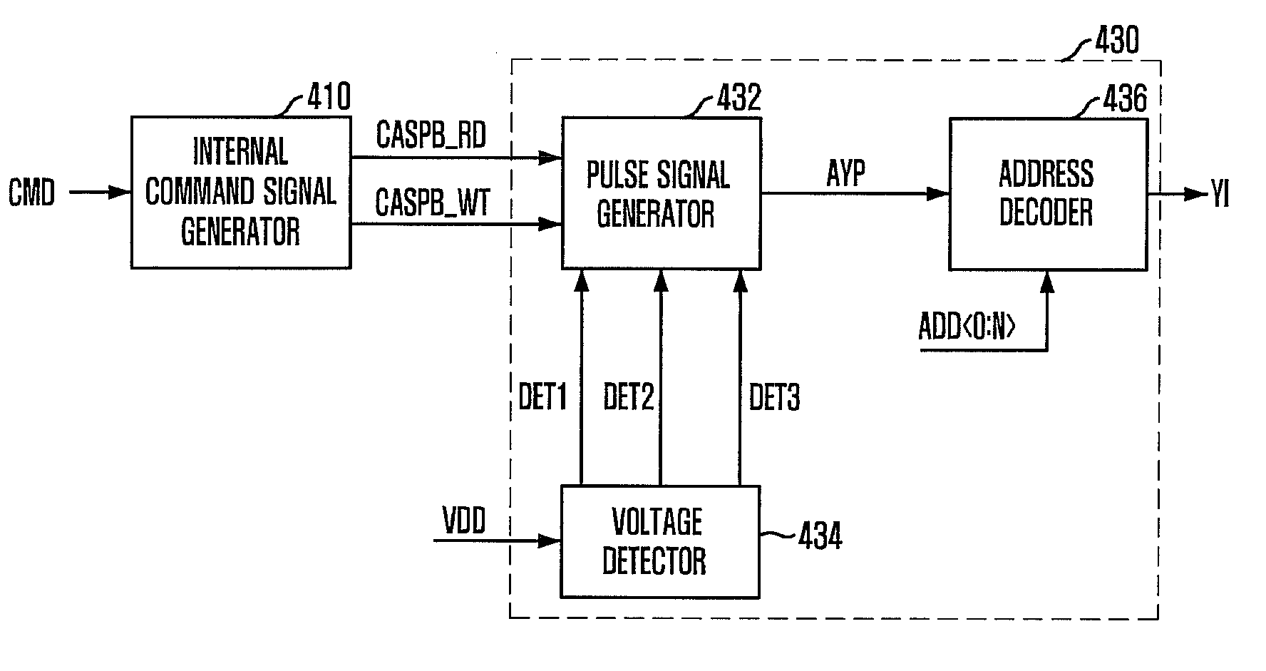
[0036]FIG. 4 is a block diagram illustrating a part of a semiconductor memory device in accordance with an embodiment of the present invention.

[0037]As shown, the semiconductor memory device includes an internal command signal generator 410 and a column selection signal generator 430.

[0038]The internal command signal generator 410 generates a read internal command signal CASPB_RD and a write internal command signal CASPB_WT in response to a column command signal CMD that is activated according to an external command signal. The column command signal CMD is a signal that is activated when a semiconductor memory device performs a read operation and a write operation. The read internal command signal CASPB_RD is a pulse signal activated when the semiconductor memory device performs a read operation, an...


PUM


Abstract

A semiconductor memory device includes a source signal generator configured to generate a source signal having a predetermined pulse width in response to a command signal, and a column selection signal generator configured to generate a column selection signal by controlling a pulse width of the source signal according to a voltage level of an external supply voltage.

Description

CROSS-REFERENCE(S) TO RELATED APPLICATIONS[0001]The present invention claims priority of Korean patent application number 10-2008-0122533, filed on Dec. 4, 2008, which is incorporated by reference in its entirety.BACKGROUND OF THE INVENTION[0002]The present invention relates to a semiconductor design technology, and more particularly, to a semiconductor memory device for generating a column selection signal that is activated in response to a read operation and a write operation.[0003]In general, a semiconductor memory device such as a Double Data Rate Synchronous DRAM (DDR SDRAM) includes more than several million memory cells for storing data and stores or outputs data according to a command from a central processing unit (CPU). That is, when the CPU requests a write operation, data is stored in a memory cell corresponding to an address inputted from the CPU. When the CPU requests a read operation, data stored in a memory cell corresponding to the input address is outputted. In oth...

Claims


Application Information

Patent Timeline
IPC IPC(8): G11C5/14G11C7/22G11C7/10G11C8/10
CPCG11C5/143G11C7/1066G11C11/4076G11C8/18G11C11/4074G11C7/22G11C7/10G11C5/14
Inventor SEO, JU-YOUNG
Owner SK HYNIX INC
Why Eureka
Try Eureka