Light emitting device with fine pattern

a light-emitting device and semiconductor technology, applied in the direction of semiconductor devices, basic electric elements, electrical appliances, etc., can solve the problems of affecting light extraction efficiency, traveling in an undesired direction or being lost in total reflection, and nitride semiconductor light-emitting devices have fundamental limitations in light extraction efficiency, so as to reduce total internal reflection and enhance light transmission efficiency

Inactive Publication Date: 2010-06-17
RENESSELAER POLYTECHNIC INST +1
View PDF4 Cites 47 Cited by
  • Summary
  • Abstract
  • Description
  • Claims
  • Application Information

AI Technical Summary

Benefits of technology

[0010]An aspect of the present invention provides a structurally improved semiconductor light emitting device to reduce total internal reflection resulting from different refractive indices between the semiconductor light emitting device and the atmosphere or an encapsulating material at the time of light extraction, and to enhance light transmission efficiency.

Problems solved by technology

However, nitride semiconductor light emitting devices have fundamental limitations in terms of light extraction efficiency.
As a result, a considerable fraction of the light generated from an active layer is totally reflected internally, thus traveling in an undesired direction or being lost in total reflection.
This inevitably impairs light extraction efficiency.
Similarly, a sapphire substrate having a refractive index of 1.78 causes low light extraction efficiency, that is, low external quantum efficiency, at the sapphire-atmosphere interface.
This low external quantum efficiency adversely affects the light emission efficiency of a semiconductor light emitting device to a significant extent.

Method used


Image

  • Light emitting device with fine pattern
  • Light emitting device with fine pattern
  • Light emitting device with fine pattern

Examples


embodiment 1

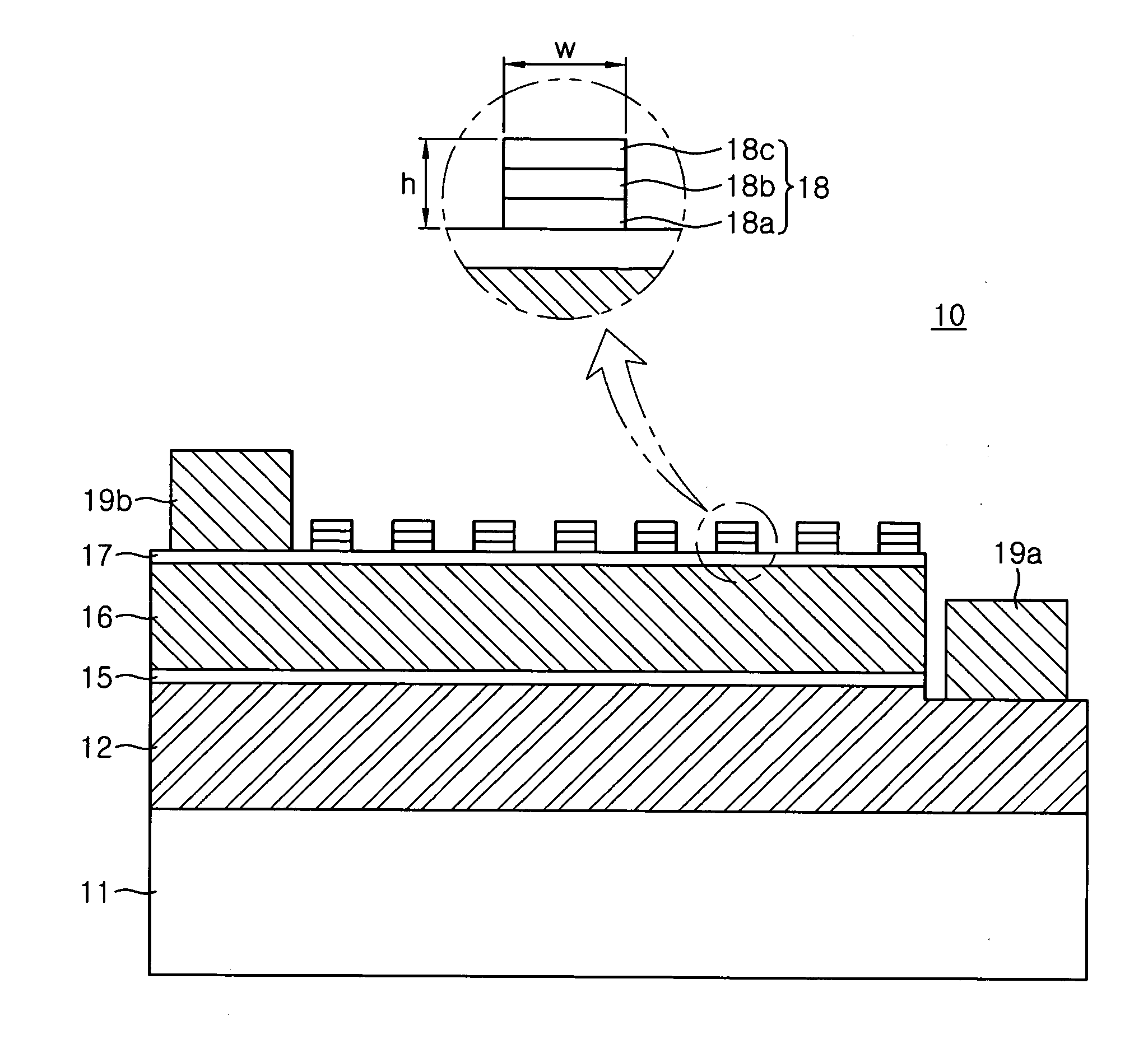
[0073]Four nitride semiconductor light emitting devices are produced. That is, an n-type GaN layer, an active layer having a InGaN / GaN MQW structure, and a p-type AlGaN / GaN layer are grown on a sapphire layer. An ITO layer having a thickness of about 200 nm is formed as a transparent electrode layer on the surface of the p-type GaN layer. Thereafter, the portion of the n-type GaN layer is exposed by mesa etching, and an n-type electrode and a p-type electrode are formed in the exposed region of the n-type GaN layer and in the region of the ITO layer, respectively.

[0074]Additionally, a fine pattern having a graded refractive index layer, proposed in the present invention, is formed on the ITO layer. This graded refractive index layer, according to this embodiment, includes the three layers of ITO / (ITO)1-x(SiO2)x, where 02, and has an overall thickness of 0.4 μm. However, the fine patterns of the four nitride semiconductor light emitting devices have different widths of 2 μm, 3 μm, 4 ...

embodiment 2

[0078]A vertical nitride semiconductor light emitting device including an InGaN / GaN active layer is produced. A fine pattern of a graded refractive index layer proposed in the present invention is formed on the surface of an n-type GaN layer. The graded refractive index layer used for this embodiment 2 has the structure of TiO2 / (TiO2)1-x(SiO2)x, where 02, and the layer of (TiO2)1-x(SiO2)x, where 0

embodiment 3

[0081]A vertical nitride semiconductor light emitting device including an InGaN / GaN active layer is produced. A fine pattern of a graded refractive index layer proposed in the present invention is formed on the surface of an n-type GaN layer. In this embodiment, the fine pattern has a hemispherical shape being 2 μm in diameter and 1 μm in height, at a period of 4 μm (see FIG. 5). The graded refractive index layer of the fine pattern has a refractive index distributed between 2.47 and 1.66 with vertical distance from the light emitting surface.


PUM


Abstract

A semiconductor light emitting device includes a semiconductor light emitting structure including first and second conductivity type semiconductor layers, and an active layer disposed therebetween, first and second electrodes connected to the first and second conductivity type semiconductor layers, respectively, and a fine pattern for light extraction, formed on a light emitting surface from which light generated from the active layer is emitted. The fine pattern for light extraction is formed as a graded refractive index layer having a refractive index which decreases with vertical distance from the light emitting surface.

Description

CROSS-REFERENCE TO RELATED APPLICATIONS[0001]The present application claims priority to U.S. Provisional Patent Application 61 / 111,177, filed Nov. 4, 2008, the disclosure of which is hereby incorporated by reference.BACKGROUND OF THE INVENTION[0002]1. Field of the Invention[0003]The present invention relates to a semiconductor light emitting device, and more particularly, to a semiconductor light emitting device having a fine pattern to enhance light extraction efficiency.[0004]2. Description of the Related Art[0005]In general, semiconductor light emitting diodes (LEDs) are in wide use as light sources for full-color displays, image scanners, various signal systems and optical communications devices. Semiconductor LEDs emit light generated from active layers using the principle of electron-hole recombination. In particular, nitride semiconductors are currently drawing a great deal of attention as the constituents of light emitting devices, which are able to cover a wide wavelength r...

Claims


Application Information

Patent Timeline
Patent Type & Authority Applications(United States)
IPC IPC(8): H01L33/00
CPCH01L33/22H01L2933/0091H01L33/44H01L33/42
Inventor KIM, JONG KYUMONT, FRANK W.NOEMAUN, AHMED N.POXSON, DAVID J.SCHUBERT, E. FREDKIM, HYUNSOOSONE, CHEOLSOO
Owner RENESSELAER POLYTECHNIC INST
Why Eureka
Try Eureka