Low power memory device with jfet device structures

a low-power memory and junction field effect transistor technology, applied in the field of memory devices and junction field effect transistor (jfet) device structures, can solve problems such as system crash, data loss, and reduced retention tim

Active Publication Date: 2010-06-17
MICRON TECH INC
View PDF11 Cites 9 Cited by
  • Summary
  • Abstract
  • Description
  • Claims
  • Application Information

AI Technical Summary

Benefits of technology

[0010]Advantages of the present invention may become apparent upon reading the following detailed description and upon reference to the drawings in which:

Problems solved by technology

If a memory cell in the memory array has a retention time less than 64 ms, the system may crash and data may be lost as bits become unreadable from the memory array.
Leakage is one possible cause of a reduced retention time.
One cause of leakage in CMOS access devices are trap states.
The state fluctuations may also result in unpredictable retention times. The erratic nature of the fluctuations result from electrons trapped along the interfaces between semiconductor and insulator (oxide), such as the gate oxide in CMOS access devices that has a gate oxide interface with the semiconductor channel.
In addition to leakage, CMOS access devices exhibit a high gate capacitance.
Thus, assuming a constant voltage supply, as the current decreases or as the capacitance increases, the speed of the device slows.
In addition to maintaining the operational speed of the access devices, a higher Vcc may result in decreased bit failures in a conventional nMOS-based DRAM cell. FIG. 2 is a scaled plot illustrating decreased bit failures in a memory array as a function of time and as a result of higher Vcc in a conventional nMOS-based DRAM memory cell.
Because of the higher voltages required for operation of CMOS access devices, scaling of the CMOS devices may be problematic.
Specifically, as the devices are scaled there may be an increase in parasitic effects between memory cells, as well as between the memory cells with other components.
Additionally, as memory cells are scaled to provide for smaller and more densely packed arrays, leakage by the CMOS access devices increases.
Furthermore, while it may be generally preferable to use a higher supply voltage in many applications the higher supply voltage results in higher power consumption.

Method used


Image

  • Low power memory device with jfet device structures
  • Low power memory device with jfet device structures
  • Low power memory device with jfet device structures

Examples


Embodiment Construction

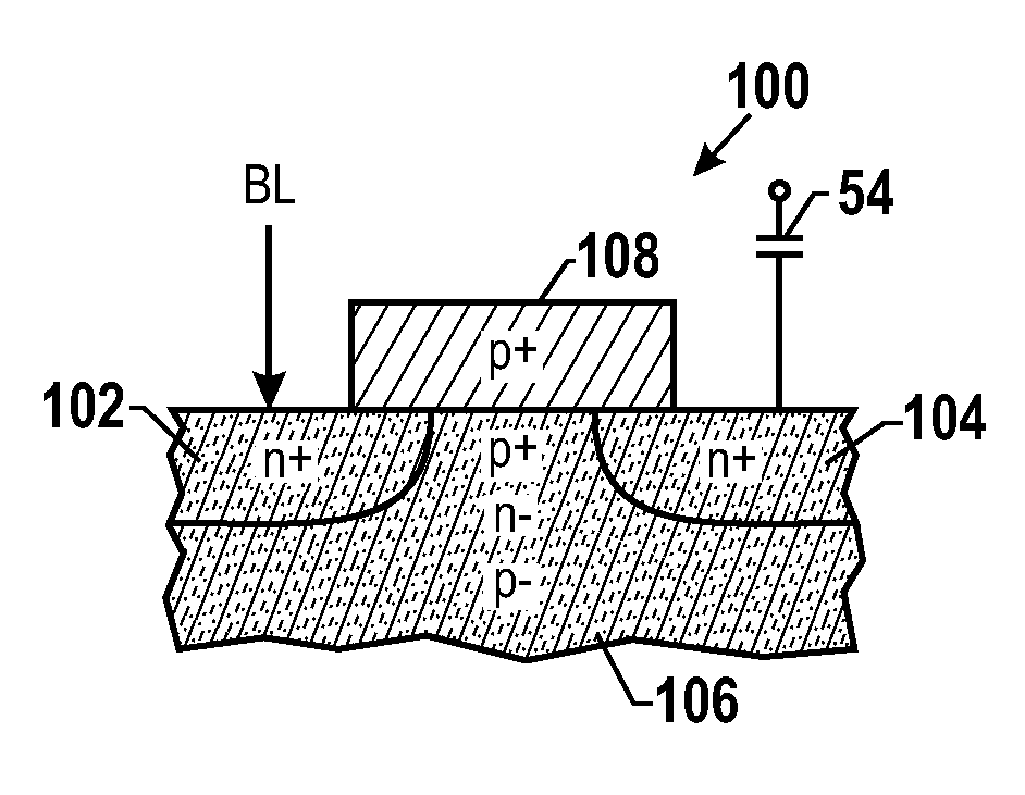
[0025]In accordance with embodiments of the present in invention, there is provided JFET device structures which may be implemented in DRAM memory arrays. Specifically, improved JFET device structure that may be used as access devices are described. Embodiments of the present invention accentuate the low power consumption characteristics of JFETs without compromises to short channel effects. As will be discussed in greater detail below, specific embodiments of JFET structures that achieve these goals include providing an enhancement mode nJFET structure, an nJFET recessed structure, a Fin-JFET structure, a RAD-Fin structure, a cylindrical structure, and an elevated source and drain Fin structure.

[0026]Conventional junction field effect transistors (JFETs) and devices using conventional JFETs may have characteristics that may limit their use in computing and logic designs. For example, JFETs are essentially two PN-junctions and, thus, have a relatively low forward bias turn on voltag...


PUM


Abstract

There is provided a low power memory device with JFET device structures. Specifically, a low power memory device is provided that includes a plurality memory cells having a memory element and a JFET access device electrically coupled to the memory element. The memory cells may be isolated using diffusion based isolation.

Description

BACKGROUND OF THE INVENTION[0001]1. Field Of The Invention[0002]The present invention relates generally to semiconductor devices and, more particularly, to memory devices and junction field-effect transistor (JFET) device structures.[0003]2. Description Of The Related Art[0004]Dynamic random access memory (DRAM) is one class of memory conventionally implemented in electronic devices. DRAM memory cells typically include an access device and a memory element. The access devices allow the transfer of charges to and from the memory elements to facilitate read and write operations in the memory device. Complementary metallic oxide semiconductor field effect transistors, commonly referred to as “CMOS” transistors, are typically used as access devices for the DRAM memory cells. The memory cells are typically arranged in a number of rows and columns to provide a memory array.[0005]DRAM devices are dynamic because once a bit of data is written into a memory cell, the data begins to degrade. ...

Claims


Application Information

Patent Timeline
Patent Type & Authority Applications(United States)
IPC IPC(8): H01L27/06H01L21/8232H01L21/762
CPCH01L21/76232H01L27/108H01L27/10844H01L27/10873H01L29/8083H01L27/10879H01L29/785H01L29/808H01L27/10876H10B12/01H10B12/05H10B12/056H10B12/053H10B12/00H10B99/00
Inventor MOULI, CHANDRA
Owner MICRON TECH INC
Why Eureka
Try Eureka