Eureka AIR delivers breakthrough ideas for toughest innovation challenges, trusted by R&D personnel around the world.

Manufacturing method of mold and method for forming liquid crystal display using the same

Inactive Publication Date: 2010-06-17
SAMSUNG DISPLAY CO LTD
View PDF6 Cites 7 Cited by
  • Summary
  • Abstract
  • Description
  • Claims
  • Application Information

AI Technical Summary

Benefits of technology

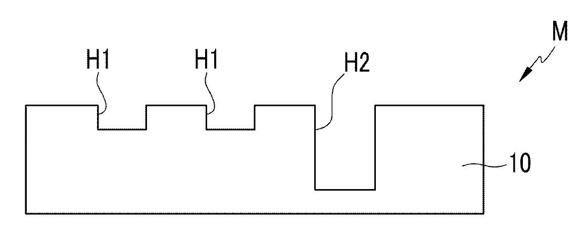
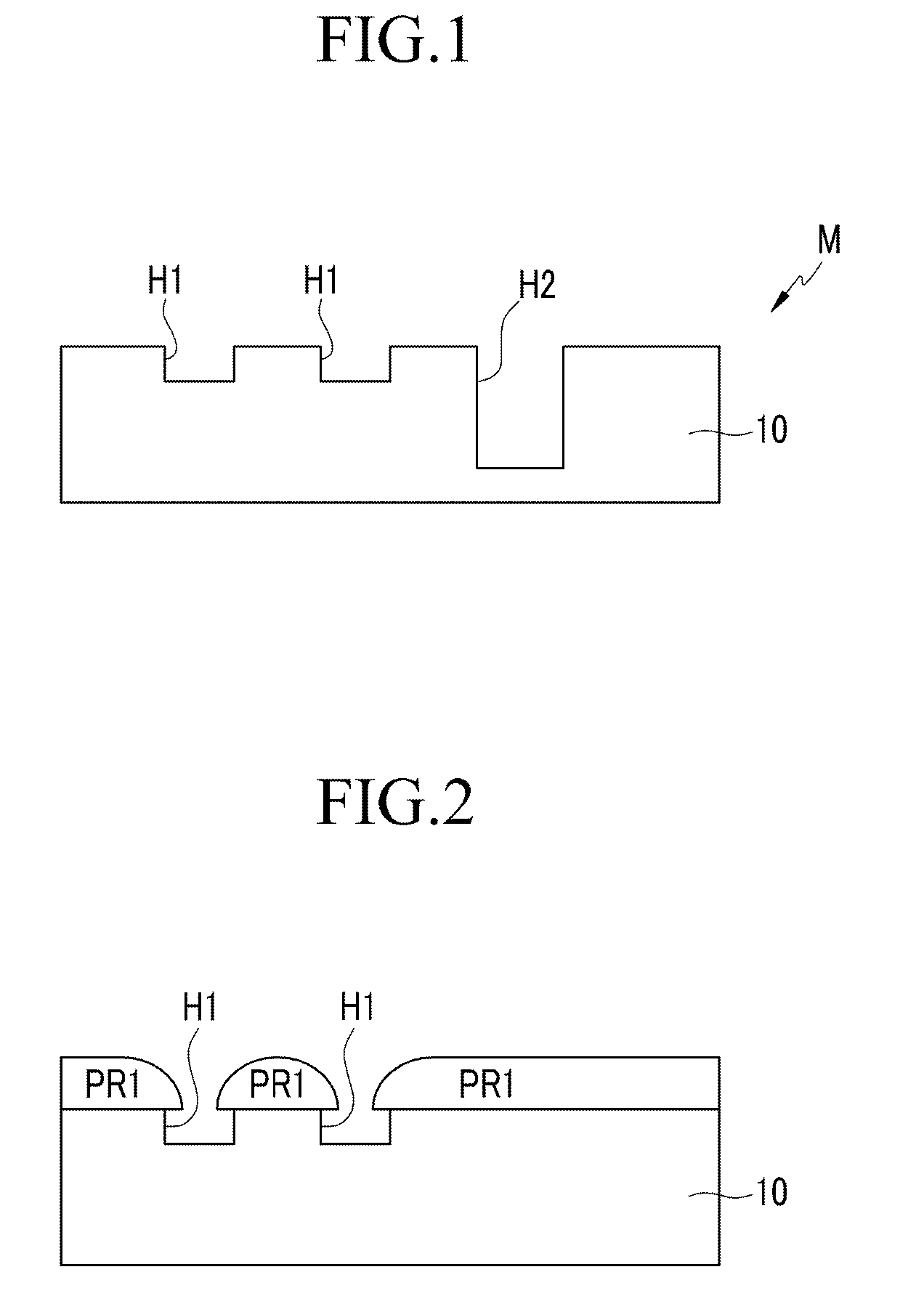
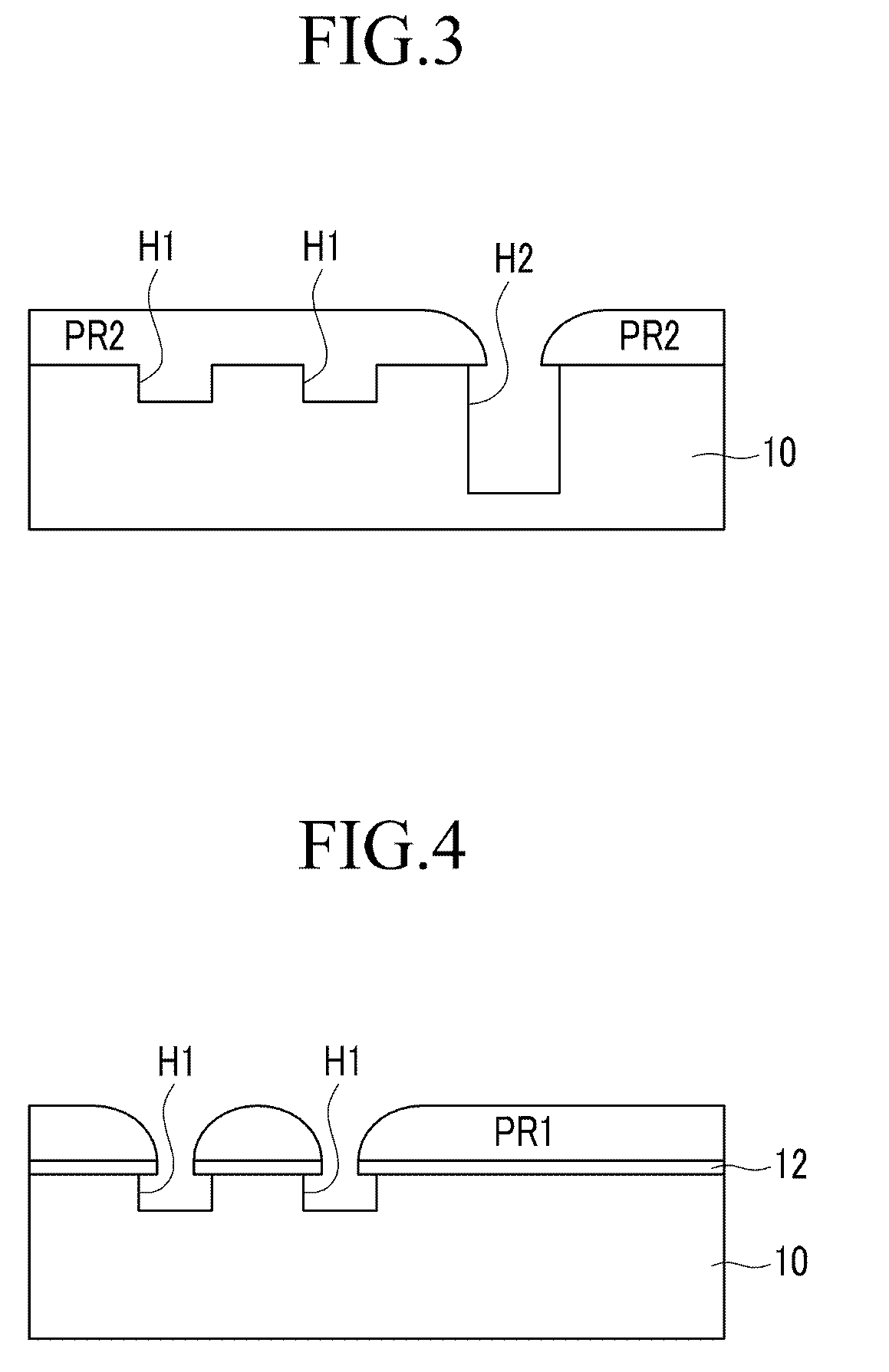
[0009]Exemplary embodiments of the present invention relate to a method of manufacturing a mold used in manufacturing LCDs. The method for manufacturing the mold may reduce the time and / or cost of manufacturing a liquid crystal display.

Problems solved by technology

However, the photolithography process suffers from several problems.
For example, the photolithography process includes highly complex steps such as the exposure and developing steps which may, for example, take an excessively long time to execute leading to delays in the execution of the photolithography process.
In addition, the photolithography process utilizes expensive equipment leading to greater costs.

Method used


Image

  • Manufacturing method of mold and method for forming liquid crystal display using the same
  • Manufacturing method of mold and method for forming liquid crystal display using the same
  • Manufacturing method of mold and method for forming liquid crystal display using the same

Examples


Embodiment Construction

[0032]The present invention is described more fully hereinafter with reference to the accompanying drawings in which exemplary embodiments of the invention are illustrated. Embodiments of the invention may, however, be embodied in many different forms and should not be construed as limited to the exemplary embodiments set forth herein. Rather, these exemplary embodiments are provided so that this disclosure is thorough, and will fully convey the scope of the invention to those skilled in the art. In the drawings, the sizes and relative sizes of layers and regions may be exaggerated for clarity. Detailed descriptions of well-known functions and structures incorporated herein may be omitted to avoid obscuring the subject matter of the embodiments. Like reference numerals in the drawings denote like elements.

[0033]It will be understood that when a first element or layer is referred to as being “on,”“connected to” or “coupled to” another element(s) or layer(s), the first element or laye...


PUM

PropertyMeasurementUnit
Coloraaaaaaaaaa
Depthaaaaaaaaaa
Photosensitivityaaaaaaaaaa

Abstract

The present invention relates to a liquid crystal display (LDC) and in particular, a method of manufacturing a mold to be used in LCDs. The method includes the following steps: forming a first photosensitive film on a substrate; etching the substrate by using the first photosensitive film as a mask to form a first groove; removing the first photosensitive film; forming a second photosensitive film covering the first groove on the substrate; and etching the substrate by using the second photosensitive film as a mask to form a second groove. The method, according to embodiments of the invention, helps reduce the time and / or cost of manufacturing a liquid crystal display.

Description

CROSS-REFERENCE TO RELATED APPLICATION[0001]This application claims priority from and the benefit of Korean Patent Application No. 10-2008-0128493, filed on Dec. 17, 2008 which is hereby incorporated by reference for all purposes as if fully set forth herein.BACKGROUND OF THE INVENTION[0002]1. Field of the Invention[0003]Embodiments of the present invention relate to a manufacturing method of a mold, and a manufacturing method of a liquid crystal display using the mold.[0004]2. Description of the Background[0005]A liquid crystal display (LCD) is one of the most commonly used flat panel displays. An LCD can include two substrates with electrodes formed thereon and a liquid crystal layer interposed between the two substrates. A voltage may be applied to the electrodes to realign liquid crystal molecules of the liquid crystal layer to regulate transmittance of light passing through the liquid crystal layer.[0006]Patterns in each layer of the LCD may be formed through a photolithography...

Claims


Application Information

Patent Timeline
IPC IPC(8): G03F7/20C23F1/02G02F1/13
CPCG03F7/0017G02F1/1333G03F7/0002
Inventor LEE, BYEONG-JINKIM, BONG-KYUNPARK, HONG-SICKJO, GUG-RAEKIM, CHANG-HOONCHOUNG, JONG-HYUNHONG, SUN-YOUNGKIM, MIN-UK
Owner SAMSUNG DISPLAY CO LTD
Why Eureka
Eureka Blog
Learn More