Method for measuring temperature of semiconductor device and apparatus for measuring temperature of semiconductor device

a technology of semiconductor devices and measurement methods, applied in the direction of instruments, heat measurement, material analysis, etc., can solve the problems of junction temperature detection errors, measurement accuracy deterioration, and inability to use the junction temperature detected by the thermal element for protection from heating, etc., and achieve the effect of high accuracy and without delay

Inactive Publication Date: 2010-06-17
THE KANSAI ELECTRIC POWER CO
View PDF10 Cites 17 Cited by
  • Summary
  • Abstract
  • Description
  • Claims
  • Application Information

AI Technical Summary

Benefits of technology

[0012]Accordingly, an object of the present invention to provide temperature measurement method and temperature measurement device for semiconductor devices capable of detecting the junction temperature of a semiconductor device with high accuracy and without delays.
[0017]According to the temperature measurement method of this invention, a temperature of a semiconductor switching element is determined by exploiting large temperature dependence of turn-OFF characteristic time of the semiconductor switching element. That is, according to the invention, the turn-OFF characteristic time measured by the second step is converted into a temperature of the semiconductor switching element based on relational characteristics between turn-OFF characteristic time of the semiconductor switching element and temperatures preliminarily measured by the first step. Thus, according to this invention, junction temperatures of semiconductor devices can be detected with high accuracy and without delay.
[0040]According to the temperature measurement device for semiconductor devices in this embodiment, the semiconductor switching element is turned OFF by the control circuit, the turn-OFF waveform is measured by the waveform measurement section, and turn-OFF characteristic time is computed from the turn-OFF characteristic time by the waveform computing section. Then, based on the preliminarily measured relational characteristics between turn-OFF characteristic time and temperatures, the temperature calculating section determines a temperature of the semiconductor switching element corresponding to the turn-OFF characteristic time inputted from the waveform computing section. Thus, according to this embodiment, junction temperatures of semiconductor devices can be detected with high accuracy and without delay.
[0058]That is, according to the invention, the turn-OFF characteristic time measured by the second step is converted into a temperature of the semiconductor switching element based on relational characteristics between turn-OFF characteristic time and temperatures preliminarily measured by the first step. Thus, according to this invention, junction temperatures of semiconductor devices can be detected with high accuracy and without delay.

Problems solved by technology

Due to this fitting of the thermal element, there have been drawbacks, for example, that measurement of the junction temperature in a current conducting state restricts electrical insulation, and moreover that the thermal element serves as a heat-absorbing source to cause errors in temperature measurement of the junction in the semiconductor device.
Furthermore, because the temperature detection by the thermal element does not follow the actual temperature increasing speed of the junction, there is a problem that the junction temperature detected by the thermal element cannot be utilized for protection from heating of the semiconductor device or the like.
Further, small temperature changes in the measurement object would cause the measurement accuracy to deteriorate.
For these reasons, the applicable range of the method to semiconductor devices to be measured has been restricted.
However, as illustrated in FIG. 12, the ON-state voltage of these bipolar semiconductor devices using wide-gap semiconductors comes to scarcely have temperature dependence when the junction temperature become 200° C. or higher.
With such a semiconductor device, there are some cases where junction temperatures of 200° C. or higher cannot be measured with high accuracy or, if they can, only can be done with considerably poor accuracy.
Also, in a case where the measurement-object semiconductor device is a high-power semiconductor device of a pressure-contact structure and where a junction temperature of this high-power semiconductor device is determined by using the temperature dependence of ON-state voltage, changes of the ON-voltage in some cases do not sufficiently reflect an average junction temperature over the entire junction surface of the measurement object.
This phenomenon occurs due to reasons, for example, that a change in pressure-contact force in the pressure-contact structure causes the contact resistance of an internal electrode to be changed, or that a measurement current to obtain an ON-voltage does not flow uniformly through the whole measurement-object semiconductor device.
Furthermore, when the current instantaneous changes, it is difficult to discriminate between a voltage change occurring from the current change and a voltage change occurring from a junction temperature change, making it impossible to determine the junction temperature with high accuracy, as a further drawback.
Since deteriorations of these component parts often progress rapidly from a certain time stage, it may occur that component abnormalities are not found by conventionally practiced periodic inspections, leading to failures of the inverter device.
With diodes or semiconductor switching elements incorporated in an inverter, abnormalities or failures often cannot be determined only by checking for resistance values between their terminals.

Method used


Image

  • Method for measuring temperature of semiconductor device and apparatus for measuring temperature of semiconductor device
  • Method for measuring temperature of semiconductor device and apparatus for measuring temperature of semiconductor device
  • Method for measuring temperature of semiconductor device and apparatus for measuring temperature of semiconductor device

Examples


first embodiment

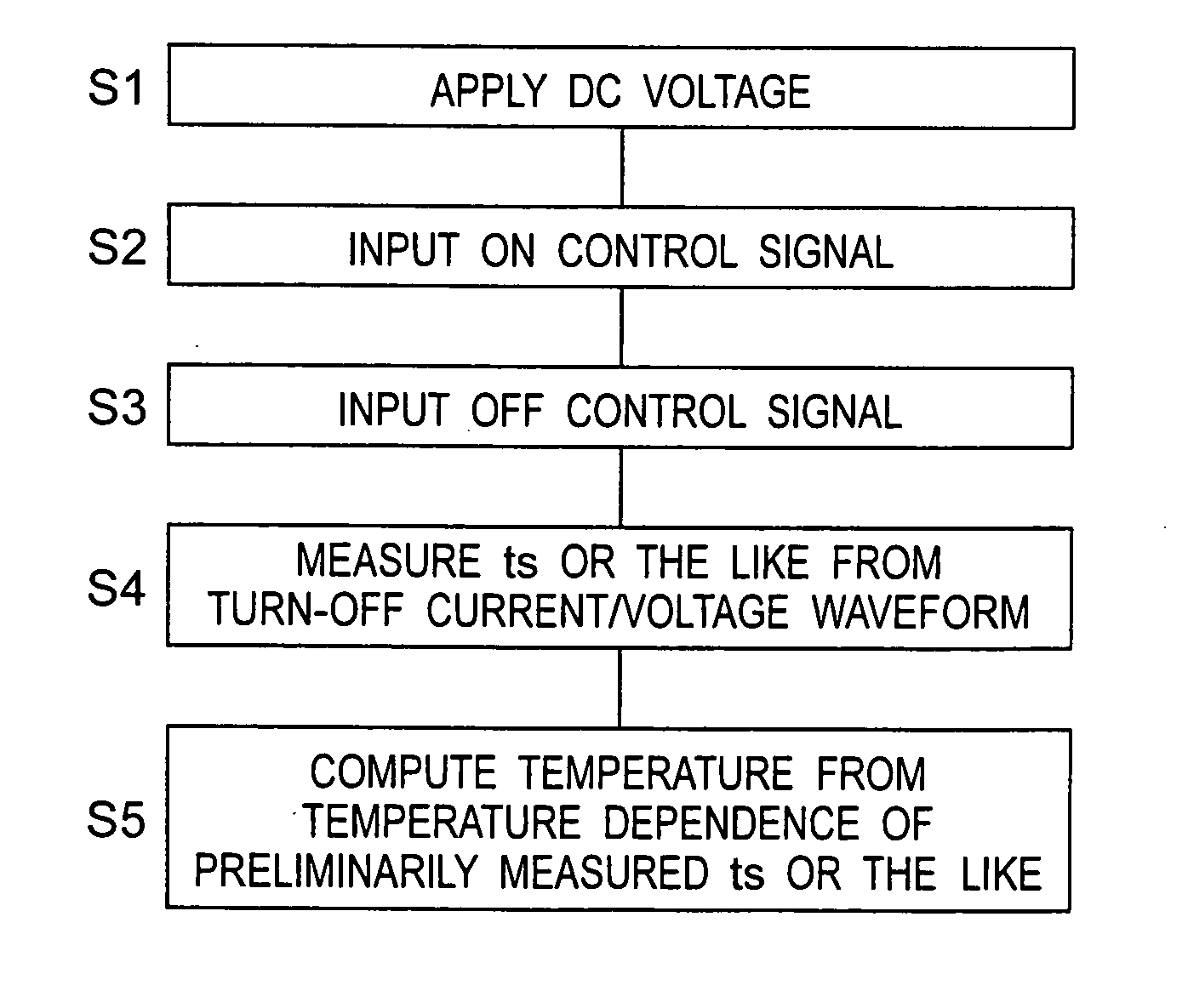
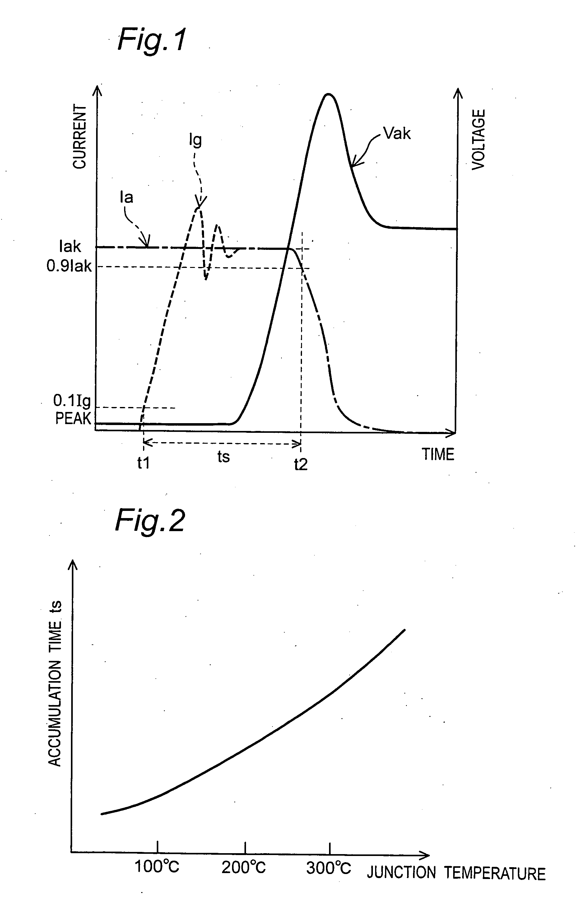
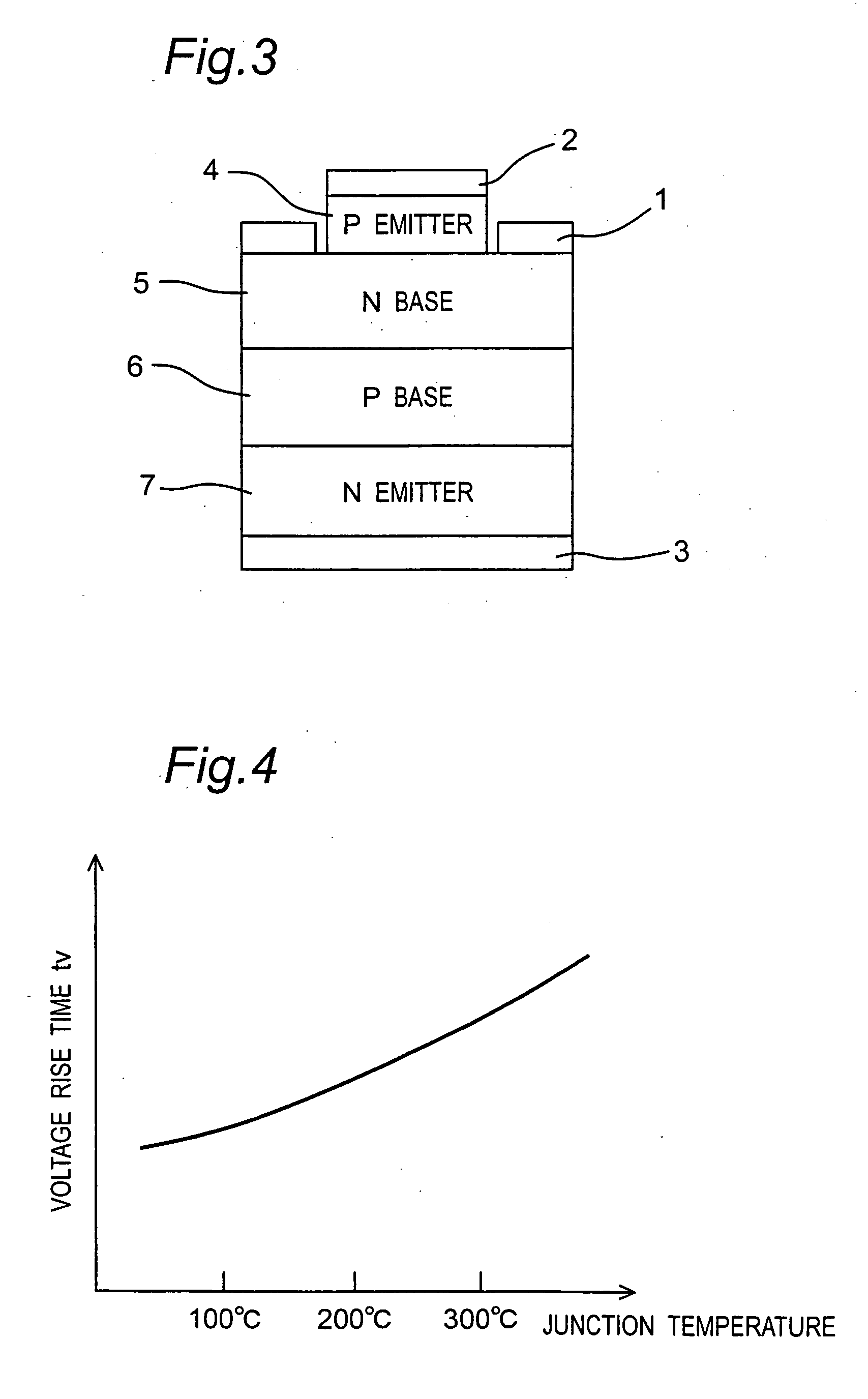
[0072]A temperature measurement method for semiconductor devices, which is a first embodiment of the invention, is described with reference to FIGS. 1 to 3. The first embodiment is a method for detecting a junction temperature of a SiC GTO (Gate Turn-Off thyristor) as an example of a semiconductor switching element without delay. FIG. 3 shows an example of the GTO structure, where reference numeral 1 denotes a gate, 2 denotes a cathode, 3 denotes an anode, 4 denotes a P emitter, 5 denotes an N base, 6 denotes a P base, and 7 denotes an N emitter.

[0073]In the GTO, with a potential of the anode 3 higher than a potential of the cathode 2, a potential of the gate 1 is set lower than the potential of the anode 3, and a forward bias voltage is applied to between the anode 3 and the gate 1. Then, a turn-ON current flows from the anode 3 to the gate 1, and moreover a current flows from the anode 3 to the cathode 2, so that the GTO turns ON, resulting in an ON state.

[0074]In this ON state, a...

second embodiment

[0088]Next, a temperature measurement device for semiconductor devices, which is a second embodiment of the invention, is described with reference to FIGS. 6 to 8.

[0089]This measurement device 30 for junction temperatures has a DC power supply 31, a capacitor 32 connected in parallel with the DC power supply 31, and a first terminal 33, a second terminal 34, a third terminal 35. Between the first terminal 33 and one end of the DC power supply 31, a load reactor 36 and a first transformer 38 as an output current measurement section are connected in series. Also, the third terminal 35 is connected to the other end of the DC power supply 31. Besides, a feedback diode 37 is connected in parallel with the load reactor 36.

[0090]Also, a voltmeter 40 as an output voltage measurement section is connected between the first terminal 33 and the third terminal 35. One end of a gate circuit 41 is connected to the first terminal 33, and the other end of the gate circuit 41 is connected to the seco...

third embodiment

[0108]Next, a thermal resistance measurement method for semiconductor devices, which is a third embodiment of the invention, is explained. The thermal resistance measurement method of this third embodiment makes use of the junction temperature measurement method of the first embodiment described above.

[0109]In this third embodiment, first, as shown by step S11 of FIG. 9, with respect to a SiC GTO (Gate Turn-Off thyristor) as an example of a semiconductor switching element that is an object of thermal resistance measurement, relational characteristics between accumulation time is and junction temperature illustrated in FIGS. 2, 4 and 5, relational characteristics between voltage rise time tv and junction temperature, and relational characteristics between current decay time ti and junction temperature are determined from such turn-OFF waveforms (gate turn-OFF current Ig, anode current Ia, anode-cathode voltage Vak) as illustrated in FIG. 1 in the same manner as described in the first...


PUM

PropertyMeasurementUnit
temperaturesaaaaaaaaaa
temperatureaaaaaaaaaa

Abstract

In the temperature measurement method for semiconductor devices, a junction temperature of a SiC GTO is determined by exploiting large temperature dependence of accumulation time ts as turn-OFF characteristic time of the SiC GTO that is a semiconductor switching element. The accumulation time ts is a time duration lasting from rise start time t1 of a gate turn-OFF current Ig until decay start time t2 of an anode current Ia. In this temperature measurement method, measured turn-OFF characteristic time is converted into a junction temperature of the SiC GTO based on relational characteristics between preliminarily measured accumulation time ts and junction temperatures.

Description

TECHNICAL FIELD[0001]The present invention relates to temperature measurement method and temperature measurement device for semiconductor switching elements such as GTOs (Gate Turn-Off thyristors).BACKGROUND ART[0002]A conventionally available method for measuring junction temperature (temperature of a junction portion) in a semiconductor device is that a thermal element such as a thermocouple is put into direct contact with a junction of the semiconductor device to measure the temperature of the junction. Another measurement method is that with preliminary examinations of temperature dependence of the ON-state voltage relative to a specified current in the semiconductor device such as shown in FIG. 11, junction temperature of the semiconductor device is determined indirectly by the value of the ON-state voltage.[0003]Also conventionally, it has been practiced that inspection of a semiconductor device incorporated in an inverter is performed by measuring resistance values between te...

Claims


Application Information

Patent Timeline
Patent Type & Authority Applications(United States)
IPC IPC(8): G01N25/18G01K3/00
CPCG01K7/346G01K7/01
Inventor ASANO, KATSUNORISUGAWARA, YOSHITAKA
Owner THE KANSAI ELECTRIC POWER CO
Why Eureka
Try Eureka