Field emission device

a field emission and emission device technology, applied in the direction of instruments, discharge tube luminescnet screens, process and machine control, etc., can solve the problems of environmental pollution, high production cost, and large amount of power consumed during reflection and transmission of light, and achieve the effect of simple structur

Active Publication Date: 2010-06-24
ELECTRONICS & TELECOMM RES INST
View PDF10 Cites 6 Cited by
  • Summary
  • Abstract
  • Description
  • Claims
  • Application Information

AI Technical Summary

Benefits of technology

[0020]The present invention is directed to a field emission device having a simple structure and capable of pulse driving and local dimming.

Problems solved by technology

However, the CCFL has a complicated configuration, and thus exacts high production costs.
Further, since a light source is disposed at a side of the CCFL, a large amount of power is consumed during reflection and transmission of light.
Further more, use of Hg causes environmental pollution, and uniformity in brightness becomes difficult to ensure as the LCD device becomes larger.
Thus, to apply such a high voltage pulse, a pulse driving high voltage power source is separately needed, which makes a driving circuit complicated, and increases production costs.

Method used


Image

  • Field emission device
  • Field emission device
  • Field emission device

Examples


Embodiment Construction

[0036]Hereinafter, the present invention will be described with reference to the accompanying drawings in detail. This invention may, however, be embodied in different forms and should not be construed as limited to the embodiments set forth herein. Rather, these embodiments are provided so that this disclosure will be thorough and complete, and will fully convey the scope of the invention to those skilled in the art. Like numbers refer to like elements throughout the specification. In the drawings, the thicknesses of layers and regions are exaggerated for clarity.

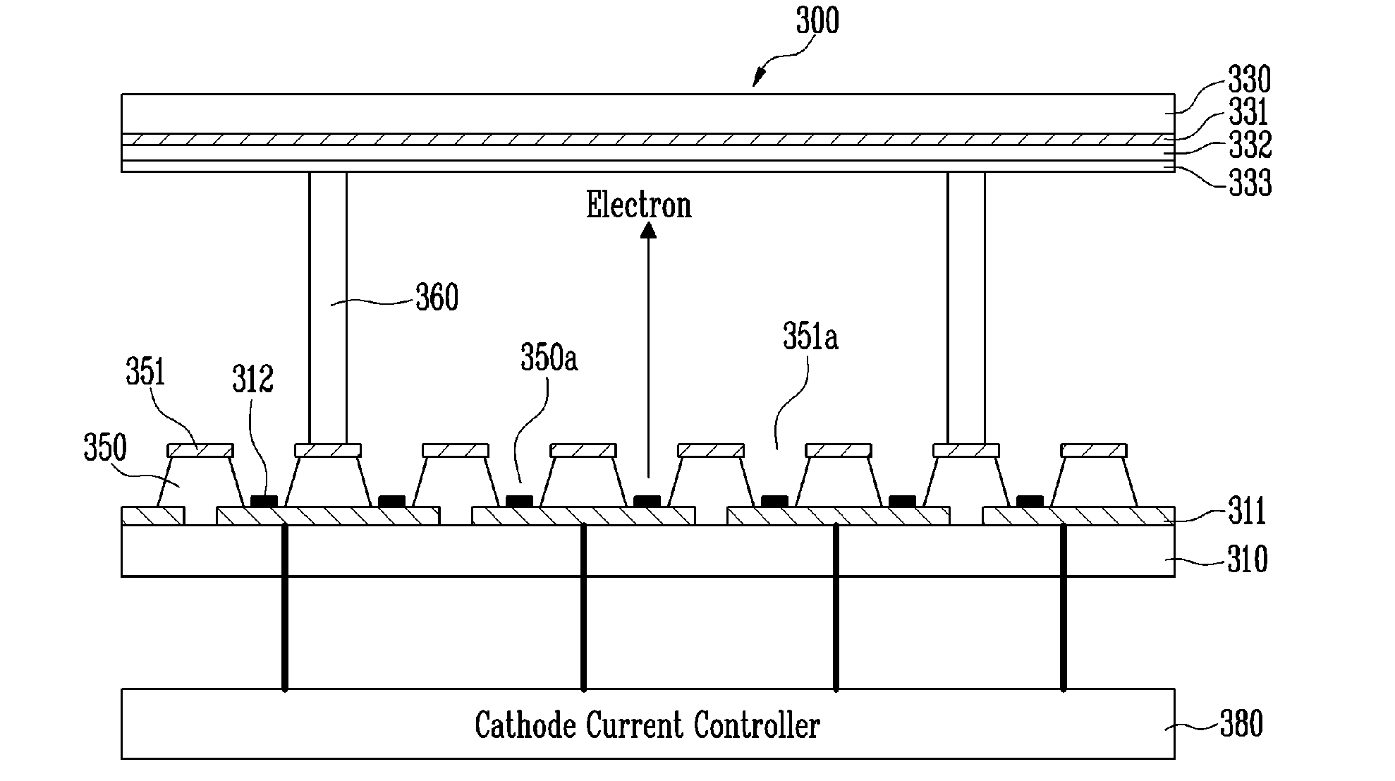
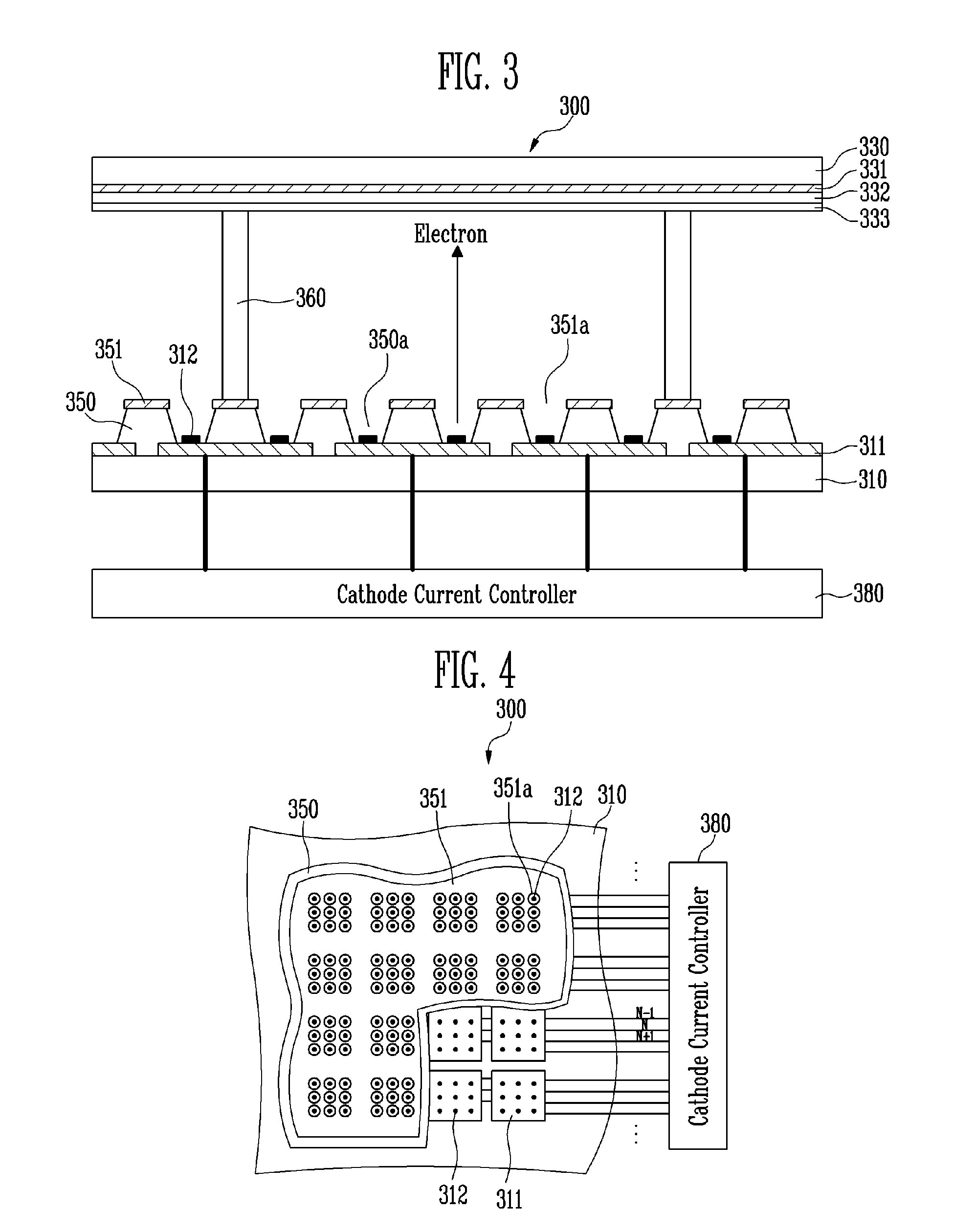
[0037]FIGS. 3 and 4 are views of a field emission device according to the present invention.

[0038]Referring to FIGS. 3 and 4, a field emission device 300 of an exemplary of the present invention includes cathode and anode substrates 310 and 330 which are spaced a predetermined distance apart to face each other, a plurality of cathode electrode blocks 311 formed to be electrically separated from each other on the cathode su...


PUM


Abstract

Provided is a field emission device having a simple structure and capable of pulse driving and local dimming. The field emission device turns a current flowing from each cathode electrode block on or off in response to a switching control signal having a very low voltage ranging from 0 to 5 V while a constant voltage is applied to an anode electrode and a gate electrode to control a field emission current. Compared with a conventional field emission device, the field emission device having a simple structure is capable of pulse driving and local dimming without using a separate pulse driving high voltage power source.

Description

CROSS-REFERENCE TO RELATED APPLICATION[0001]This application claims priority to and the benefit of Korean Patent Application No. 10-2008-0129659, filed Dec. 18, 2008, the disclosure of which is incorporated herein by reference in its entirety.BACKGROUND[0002]1. Field of the Invention[0003]The present invention relates to a field emission device, and more particularly, to a field emission device having a simple structure and capable of pulse driving and local dimming.[0004]2. Discussion of Related Art[0005]Generally, in a field emission device, a cathode substrate having a field emitter and an anode substrate having a fluorescent layer are spaced a predetermined distance apart to face each other and vacuum-packaged, and electrons emitted from the field emitter are collided with the fluorescent layer of the anode substrate to emit light due to cathode luminescence of the fluorescent layer.[0006]In recent times, field emission devices have received great attention as lighting devices c...

Claims


Application Information

Patent Timeline
Patent Type & Authority Applications(United States)
IPC IPC(8): H05B37/02H01J1/62
CPCG09G3/22G09G3/3406G09G2320/0633H05B41/14G09G2330/025G09G2330/04G09G2320/064H01J1/30H01J2201/30469
Inventor JEONG, JIN WOOSONG, YOON HOKIM, DONG ILKANG, JUN TAEKIM, JI SEON
Owner ELECTRONICS & TELECOMM RES INST
Why Eureka
Try Eureka