Semiconductor device including insulated gate bipolar transistor and diode

a technology of insulated gate bipolar transistor and diode, which is applied in the direction of diodes, electronic switching, pulse techniques, etc., can solve the problems of inverter circuit malfunction, direct-current loss increase, forward voltage vf increase, etc., and achieve the effect of reducing the fwd

Active Publication Date: 2010-06-24
DENSO CORP
View PDF17 Cites 91 Cited by
  • Summary
  • Abstract
  • Description
  • Claims
  • Application Information

AI Technical Summary

Benefits of technology

[0018]In the semiconductor device according to the second aspect of the present i

Problems solved by technology

When a spike-shaped snapback generates in the forward voltage Vf, the inverter circuit may malfunction.
I

Method used


Image

  • Semiconductor device including insulated gate bipolar transistor and diode
  • Semiconductor device including insulated gate bipolar transistor and diode
  • Semiconductor device including insulated gate bipolar transistor and diode

Examples


first embodiment

[0051]A semiconductor device 100 according to a first embodiment of the present invention will be described with reference to FIG. 5 to FIG. 7.

[0052]The semiconductor device 100 includes a semiconductor substrate 10 having first and second surfaces opposing each other. The semiconductor device 100 includes a vertical IGBT and a vertical FWD coupled in anti-parallel to each other. The IGBT has a plurality of gate electrodes 12 adjacent to the first surface of the semiconductor substrate 10. The semiconductor device 100 can be used, for example, as a power switching device for an extra-high voltage (EHV) inverter module. In the following description, the same reference numerals are given to components same as the components illustrated in FIG. 1 and FIG. 2. In addition, the thickness direction of the semiconductor substrate is expressed as the thickness direction, a direction perpendicular to the thickness direction is expressed as the perpendicular direction, and one direction in the...

second embodiment

[0088]A semiconductor device 100 according to a second embodiment of the present invention will be described with reference to FIG. 10. A cross-sectional view of the semiconductor device 100 illustrated in FIG. 10 corresponds to a cross section taken along line X-X in FIG. 5.

[0089]Because the semiconductor device according to the present embodiment have many portions in common with the semiconductor device according to the first embodiment, a description of the common portions will be omitted and different portions will be mainly described. In the following description, the same reference numerals are given to components same as the components described in the first embodiment.

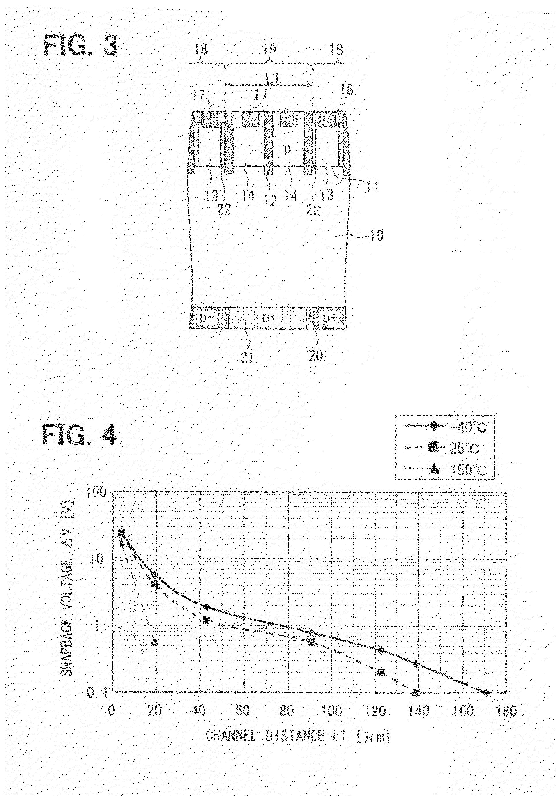
[0090]In the present embodiment, a plurality of portions in the base regions 11 arranged in the first direction extends from the main section 30 of the semiconductor substrate 10 to a part of the outer peripheral section 50, as illustrated in FIG. 10. A snapback of the FWD can be restricted by using a portion ...

third embodiment

[0107]A semiconductor device 100 according to a third embodiment of the present invention will be described with reference to FIG. 11 to FIG. 13. Because the semiconductor device 100 according to the present embodiment has many portions in common with the semiconductor device 100 according to the first embodiment or the semiconductor device 100 according to the second embodiment, a description of the common portions will be omitted and different portions will be mainly described. In the following description, the same reference numerals are given to components same as the components described in the first embodiment and the second embodiment.

[0108]In the semiconductor device 100 illustrated in FIG. 11, the section 51 in the outer peripheral section 50 includes a sense section 51a. A section where the IGBT and the FWD are disposed is expressed as an active device section. The active device section has a first area along the first surface of the semiconductor substrate 10. The sense s...


PUM


Abstract

A semiconductor device includes a vertical IGBT and a vertical free-wheeling diode in a semiconductor substrate. A plurality of base regions is disposed at a first-surface side portion of the semiconductor substrate, and a plurality of collector regions and a plurality of cathode regions are alternately disposed in a second-surface side portion of the semiconductor substrate. The base regions include a plurality of regions where channels are provided when the vertical IGBT is in an operating state. The first-side portion of the semiconductor substrate include a plurality of IGBT regions each located between adjacent two of the channels, including one of the base regions electrically coupled with an emitter electrode, and being opposed to one of the cathode regions. The IGBT regions include a plurality of narrow regions and a plurality of wide regions.

Description

CROSS REFERENCE TO RELATED APPLICATIONS[0001]The present application is based on and claims priority to Japanese Patent Applications No. 2008-328426 filed on Dec. 24, 2008, and No. 2009-259135 filed on Nov. 12, 2009, the contents of which are incorporated in their entirety herein by reference.BACKGROUND OF THE INVENTION[0002]1. Field of the Invention[0003]The present invention relates to a semiconductor device including a vertical insulated gate bipolar transistor (vertical IGBT) and a vertical free-wheeling diode (vertical FWD) formed in one semiconductor substrate.[0004]2. Description of the Related Art[0005]In a conventional reverse-conducting IGBT device (RC-IGBT device), a vertical FWD and a vertical IGBT are formed in one semiconductor substrate as described, for example, in US 2005 / 0017290 A (corresponding to JP-A-2005-57235) and US 2008 / 0048295 A (corresponding to JP-A-2008-53648).[0006]In the RC-IGBT device, an anode electrode of the FWD and an emitter electrode of the IGBT...

Claims


Application Information

Patent Timeline
IPC IPC(8): H03K17/60H01L27/06
CPCH01L27/0664H01L29/0619H01L29/0834H03K17/145H01L29/7397H03K17/0828H01L29/7395
Inventor TSUZUKI, YUKIOTANABE, HIROMITSUKOUNO, KENJI
Owner DENSO CORP
Why Eureka
Try Eureka