Exposure apparatus, exposure method, and device manufacturing method

Active Publication Date: 2010-06-24
NIKON CORP
View PDF100 Cites 40 Cited by
  • Summary
  • Abstract
  • Description
  • Claims
  • Application Information

AI Technical Summary

Benefits of technology

[0019]According to the method, it becomes possible

Problems solved by technology

When the size of the wafer becomes as large as 450 mm, while the number of dies (chips) output from a single wafer increases, a risk also occurs of throughput deceasing due to an increase in the time required to perform an exposure process on a single wafer.
However, applying the exposure apparatus using the con

Method used


Image

  • Exposure apparatus, exposure method, and device manufacturing method
  • Exposure apparatus, exposure method, and device manufacturing method
  • Exposure apparatus, exposure method, and device manufacturing method

Examples


first embodiment

A First Embodiment

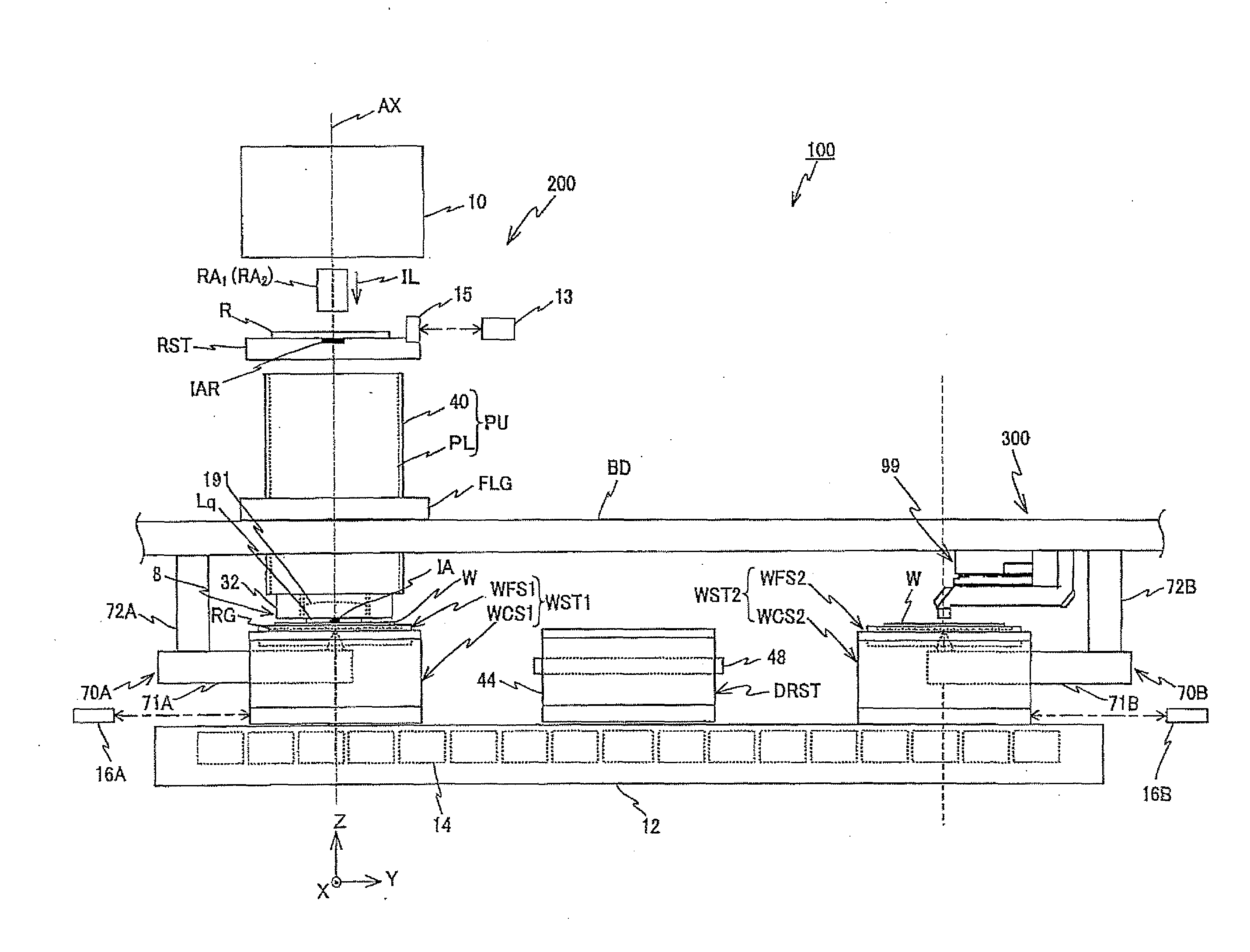
[0069]A first embodiment of the present invention will be described below, with reference to FIGS. 1 to 25F.

[0070]FIG. 1 schematically shows a configuration of an exposure apparatus 100 in the first embodiment. Exposure apparatus 100 is a projection exposure apparatus by the step-and-scan method, or a so-called scanner. As it will be described later, a projection optical system PL is arranged in the embodiment, and in the description below, a direction parallel to an optical axis AX of projection optical system PL will be described as the Z-axis direction, a direction within a plane orthogonal to the Z-axis direction in which a reticle and a wafer are relatively scanned will be described as the Y-axis direction, a direction orthogonal to the Z-axis and the Y-axis will be described as the X-axis direction, and rotational (inclination) directions around the X-axis, the Y-axis, and the Z-axis will be described as θx, θy, and θz directions, respectively. The same can b...

second embodiment

A Second Embodiment

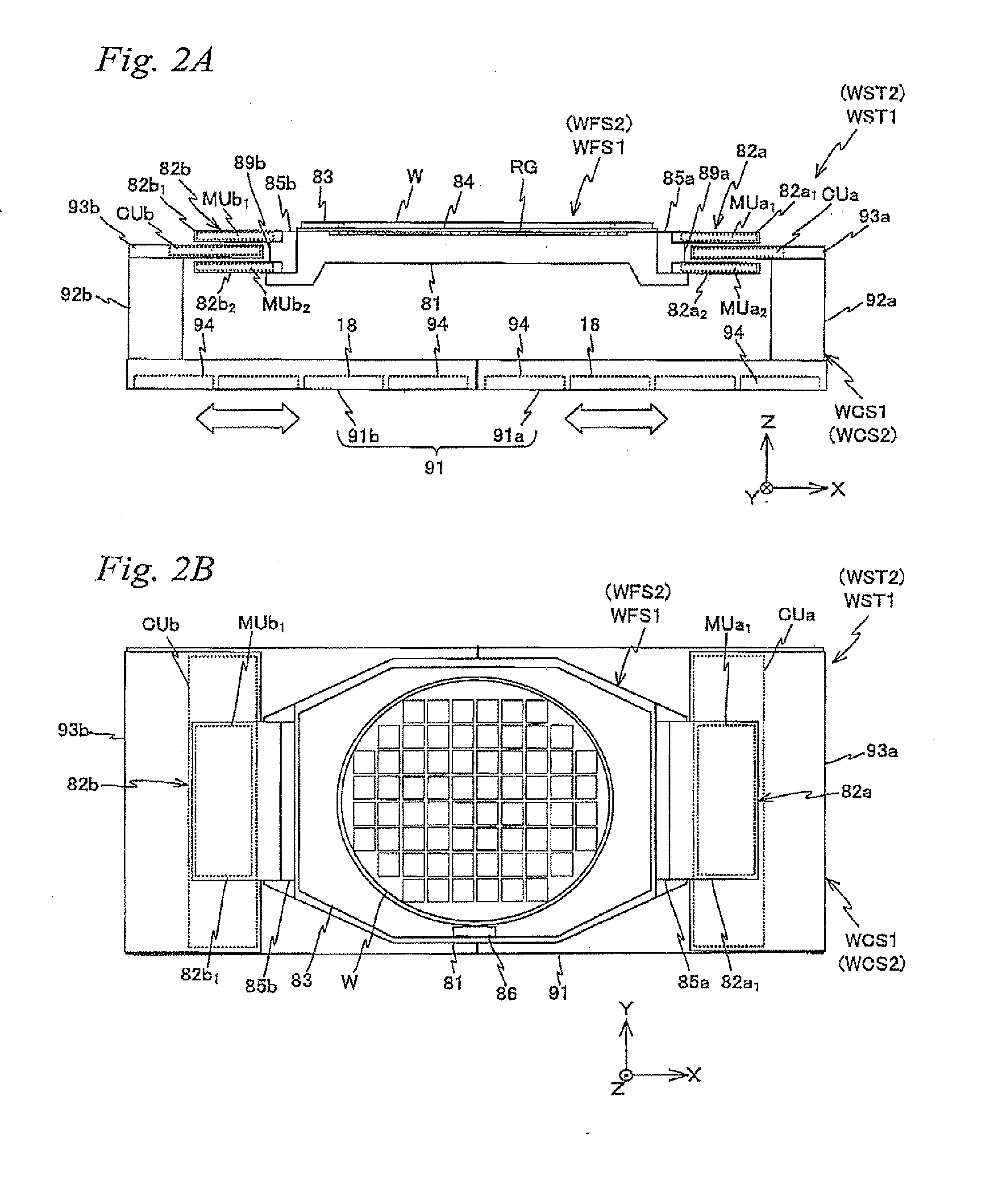
[0247]Hereinafter, a second embodiment of the present invention will be described, with reference to FIGS. 26 to 45. Here, the same reference numerals will be used for the same or similar sections as in the first embodiment previously described, and a detailed description thereabout will be simplified or omitted.

[0248]FIG. 26 shows a schematic configuration of exposure apparatus 1100 of the second embodiment in a planar view, and FIG. 27 schematically shows a side view of exposure apparatus 1100 in FIG. 26. Further, FIG. 29A shows a side view of a wafer stage which exposure apparatus 1100 is equipped with when viewed from the −Y direction, and FIG. 29B shows a planar view of the wafer stage. Further, FIG. 30A, shows an extracted planar view of a coarse movement stage, and FIG. 30B is a planar view in a state where the coarse movement stage is separated into two sections.

[0249]Exposure apparatus 1100 is a projection exposure apparatus by the step-and-scan method, o...


PUM


Abstract

When a wafer on a fine movement stage supported by a coarse movement stage is exposed via a projection optical system with an illumination light at an exposure station, a position of the fine movement stage within an XY plane is measured with good precision by a measurement system. Further, when an alignment to a wafer on a fine movement stage supported by a coarse movement stage is performed at a measurement station, a position of the fine movement stage within an XY plane is measured with good precision by a measurement system.

Description

CROSS-REFERENCE TO RELATED APPLICATIONS[0001]This non-provisional application claims the benefit of Provisional Application No. 61 / 139,314 filed Dec. 19, 2008, Provisional Application No. 61 / 213,376 filed Jun. 2, 2009, and Provisional Application No. 61 / 272,398 filed Sep. 21, 2009, the disclosures of which are hereby incorporated herein by reference in its entirety.BACKGROUND OF THE INVENTION[0002]1. Field of the Invention[0003]The present invention relates to exposure apparatuses, exposure methods, and device manufacturing methods, and more particularly to an exposure apparatus and an exposure method which are used in a lithography process to produce electronic devices such as a semiconductor device and the like, and a device manufacturing method which uses the exposure apparatus or the exposure method.[0004]2. Description of the Background Art[0005]Conventionally, in a lithography process for manufacturing electron devices (microdevices) such as semiconductor devices (such as inte...

Claims


Application Information

Patent Timeline
IPC IPC(8): G03B27/58
CPCG03F7/70341G03F7/70775G03F7/70733H01L21/0273
Inventor SHIBAZAKI, YUICHI
Owner NIKON CORP
Why Eureka
Try Eureka