Bonding IC die to TSV wafers

a technology of die-to-die bonding and tsv wafers, which is applied in the direction of electrical equipment, semiconductor devices, semiconductor/solid-state device details, etc., can solve the problems of complex process flow, yield loss, and die-to-die bonding via bumps, and achieves significant simplified assembly flow, reduced scratching, and high yield

Active Publication Date: 2010-06-24
TEXAS INSTR INC
View PDF14 Cites 78 Cited by
  • Summary
  • Abstract
  • Description
  • Claims
  • Application Information

AI Technical Summary

Benefits of technology

[0006]Disclosed embodiments provide solutions to the problem of thinning a TSV comprising wafer to expose the TSVs for electrical access from the bottom of the wafer when singulated dies or stacks of singulated IC dies are bonded on the IC die formed on top (i.e. circuit side) of the TSV comprising wafer. By thinning the TSV comprising wafer after the singulated IC die is attached to the top side of the wafer, the assembly flow is significantly simplified and as a result the yield is higher and the scratching is reduced. Moreover, jointing to thick (pre-backgrind) wafers reduces warpage / bow which reduces the contact resistance of the joints, and as a result improves circuit performance and reliability.

Problems solved by technology

Problems with this conventional sequential stacked die assembly technique include a complicated process flow.
There are also difficulties with die-to die jointing via bumps because the first IC die mounted that is on the package substrate may have significant warpage / bow.
In addition, since both IC die are thinned and the top active circuit comprising sides are exposed during assembly, die handling is generally difficult and can result in yield loss due to cracked IC die or scratching of the IC die.
The Inventors have recognized that conventional sequential stacked IC die assembly techniques for forming die-wafer stacks involve handling thin (post-backgrind) wafers involve complicated process flows that generally result in significant yield loss and scratching.
Moreover, thin IC die are subject to warpage / bow which complicates jointing and can result in high resistance joints which can lead to degraded circuit performance and / or reliability problems.

Method used


Image

  • Bonding IC die to TSV wafers
  • Bonding IC die to TSV wafers
  • Bonding IC die to TSV wafers

Examples


Embodiment Construction

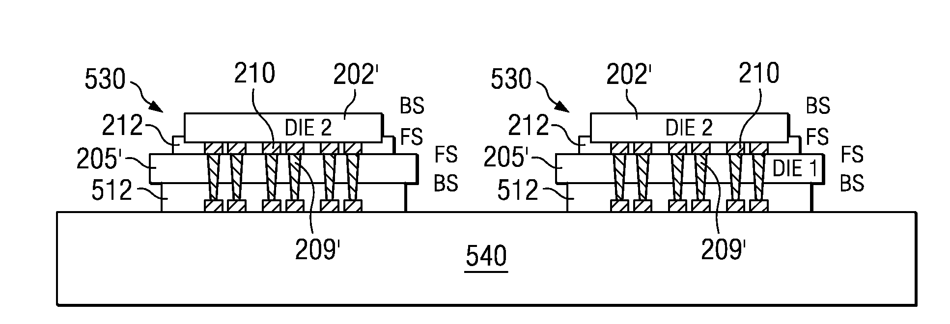
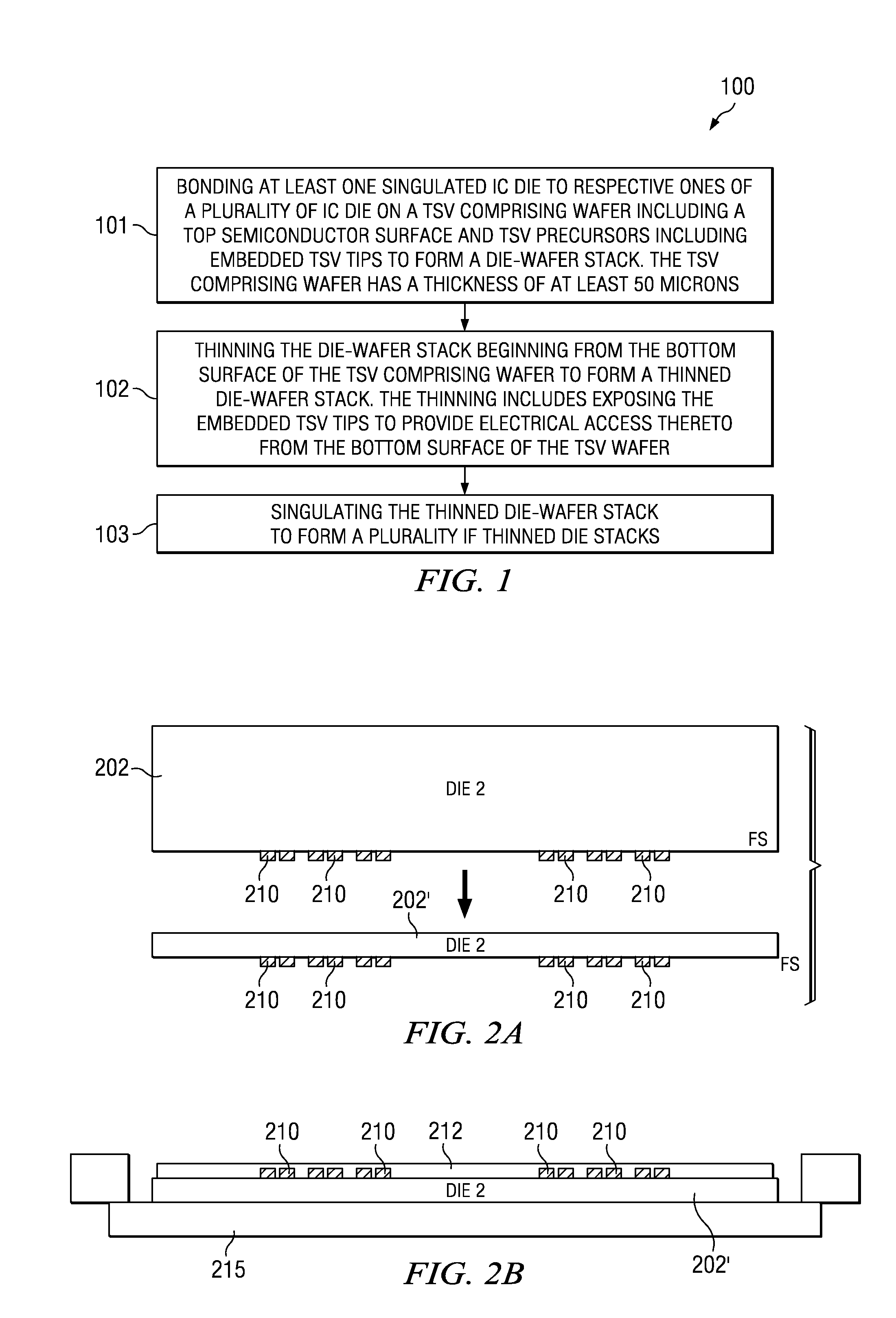
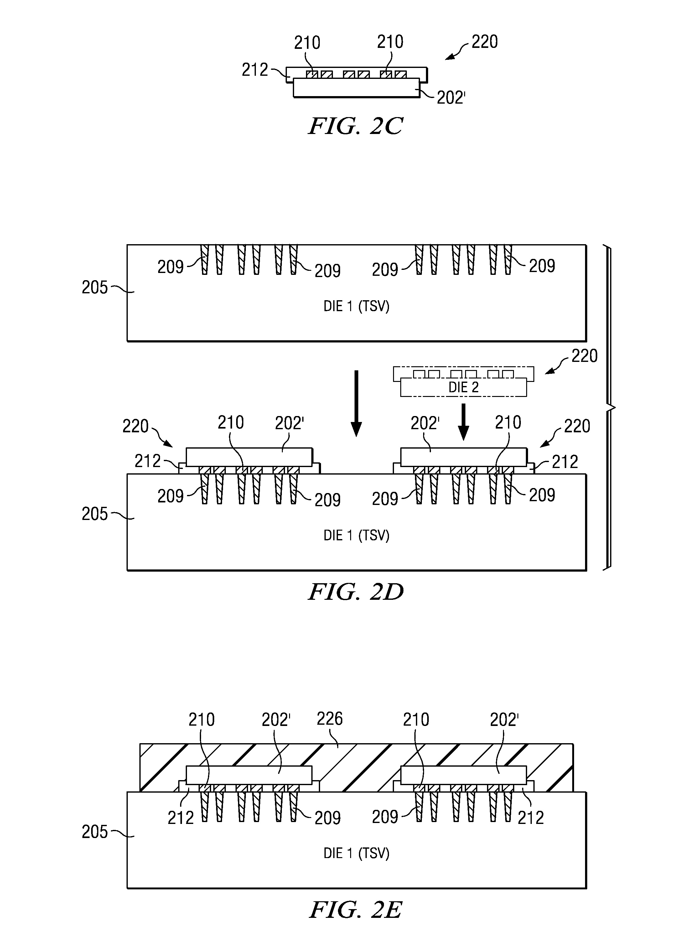
[0012]Disclosed embodiments are described with reference to the attached figures, wherein like reference numerals are used throughout the figures to designate similar or equivalent elements. The figures are not drawn to scale and they are provided merely to illustrate the disclosed embodiments. Several disclosed aspects are described below with reference to example applications for illustration. It should be understood that numerous specific details, relationships, and methods are set forth to provide a full understanding of the disclosed embodiments. One having ordinary skill in the relevant art, however, will readily recognize that embodiments of the invention can be practiced without one or more of the specific details or with other methods. In other instances, well-known structures or operations are not shown in detail to avoid obscuring the disclosure. The disclosed embodiments are not limited by the illustrated ordering of acts or events, as some acts may occur in different or...


PUM


Abstract

A method for bonding IC die to TSV wafers includes bonding at least one singulated IC die to respective ones of a plurality of IC die on a TSV wafer that includes a top semiconductor surface and TSV precursors including embedded TSV tips to form a die-wafer stack. The die-wafer stack is thinned beginning from the bottom surface of the TSV wafer to form a thinned die-wafer stack. The thinning includes exposing the embedded TSV tips to provide electrical access thereto from the bottom surface of the TSV wafer. The thinned die-wafer stack can be singulated to form a plurality of thinned die stacks.

Description

CROSS REFERENCE TO RELATED APPLICATIONS[0001]This application claims the benefit of Provisional Application Ser. No. 61 / 139,070 entitled “Stacked F2F FCSP flow using Single carrier with post-die stacking TSV tip exposure,” filed Dec. 19, 2008, which is herein incorporated by reference in its entirety.FIELD[0002]Disclosed embodiments relate to integrated circuit (IC) assembly processing, and more particularly to die-to-wafer bonding, where the wafer is a TSV comprising wafer.BACKGROUND[0003]In order to stack IC die in a face-to-face manner using standard flip-chip assembly techniques, the assembly is conventionally performed in a sequential manner by bonding a first thinned IC die then a second thinned IC die (e.g., 25 to 150 μm) onto a package substrate (e.g., PCB). In a typical arrangement, the first IC die can be a TSV comprising die that is mounted face (i.e. active circuit side) up on the surface of a package substrate where the TSVs form joints with pads on the package substrat...

Claims


Application Information

Patent Timeline
Patent Type & Authority Applications(United States)
IPC IPC(8): H01L21/98
CPCH01L21/56H01L2924/1461H01L21/76898H01L23/3107H01L24/02H01L24/12H01L24/16H01L24/81H01L24/94H01L24/97H01L25/0652H01L25/50H01L2224/13009H01L2224/13099H01L2224/274H01L2224/81203H01L2224/81801H01L2224/81894H01L2224/83191H01L2924/01005H01L2924/01014H01L2924/01029H01L2924/01082H01L2924/014H01L2924/14H01L2924/19041H01L2924/01006H01L2924/01033H01L24/27H01L21/6835H01L2924/00H01L24/13H01L2224/0401H01L2224/11002H01L2224/73104H01L2224/94H01L2224/97H01L2224/81
Inventor TAKAHASHI, YOSHIMIMURTUZA, MASOODDUNNE, RAJIVCHAUHAN, SATYENDRA
Owner TEXAS INSTR INC
Why Eureka
Try Eureka