Method of manufacturing electromagnetic interference (EMI) shielding filter for plasma display panel and EMI shielding filter for plasma display panel using the same

a technology of electromagnetic interference and shielding filter, which is applied in the manufacture of electrode systems, electric discharge tubes/lamps, instruments, etc., can solve the problems of increasing the production cost of plasma display devices, plasma display devices often suffer from high-level generation of electromagnetic waves, etc., and achieves the effect of reducing production costs and simplifying production processes

Inactive Publication Date: 2010-07-01
SAMSUNG SDI CO LTD
View PDF8 Cites 5 Cited by
  • Summary
  • Abstract
  • Description
  • Claims
  • Application Information

AI Technical Summary

Benefits of technology

[0008]Aspects of the present invention provide a method of manufacturing an electromagnetic interference (EMI) shielding filter for a plasma display panel and an EMI shielding filter for plasma display panel using the same which are capable of simplifying production processes and reducing producti...

Problems solved by technology

Plasma display devices often suffer from high-level generation of electromagnetic waves in the plasma display panel during a driving process ther...

Method used


Image

  • Method of manufacturing electromagnetic interference (EMI) shielding filter for plasma display panel and EMI shielding filter for plasma display panel using the same
  • Method of manufacturing electromagnetic interference (EMI) shielding filter for plasma display panel and EMI shielding filter for plasma display panel using the same
  • Method of manufacturing electromagnetic interference (EMI) shielding filter for plasma display panel and EMI shielding filter for plasma display panel using the same

Examples


Embodiment Construction

[0021]In the following detailed description, only certain exemplary embodiments of the present invention are shown and described, by way of illustration. As those skilled in the art would recognize, the invention may be embodied in many different forms and should not be construed as being limited to the embodiments set forth herein. Like reference numerals designate like elements throughout the specification.

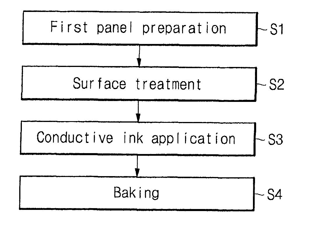
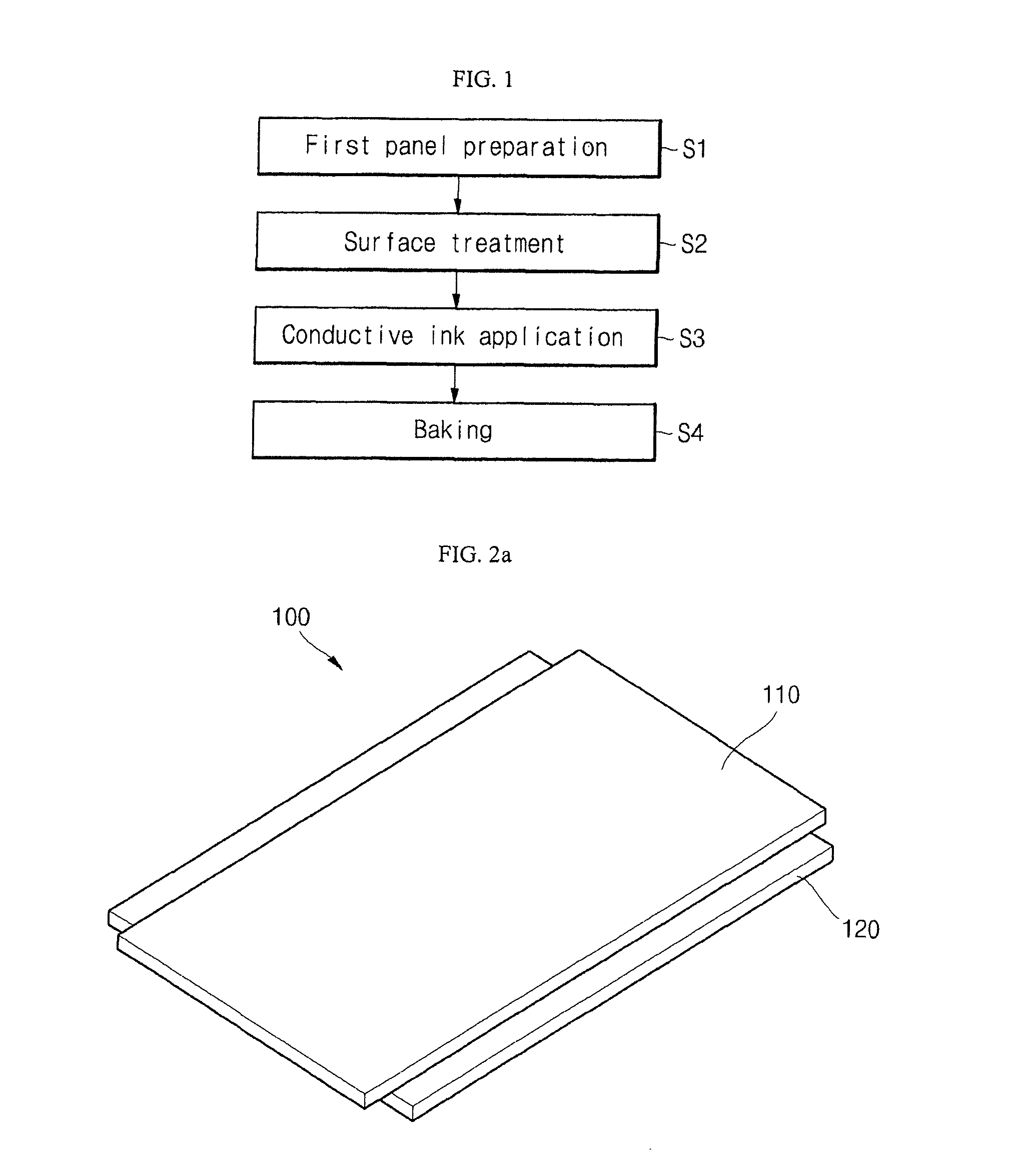
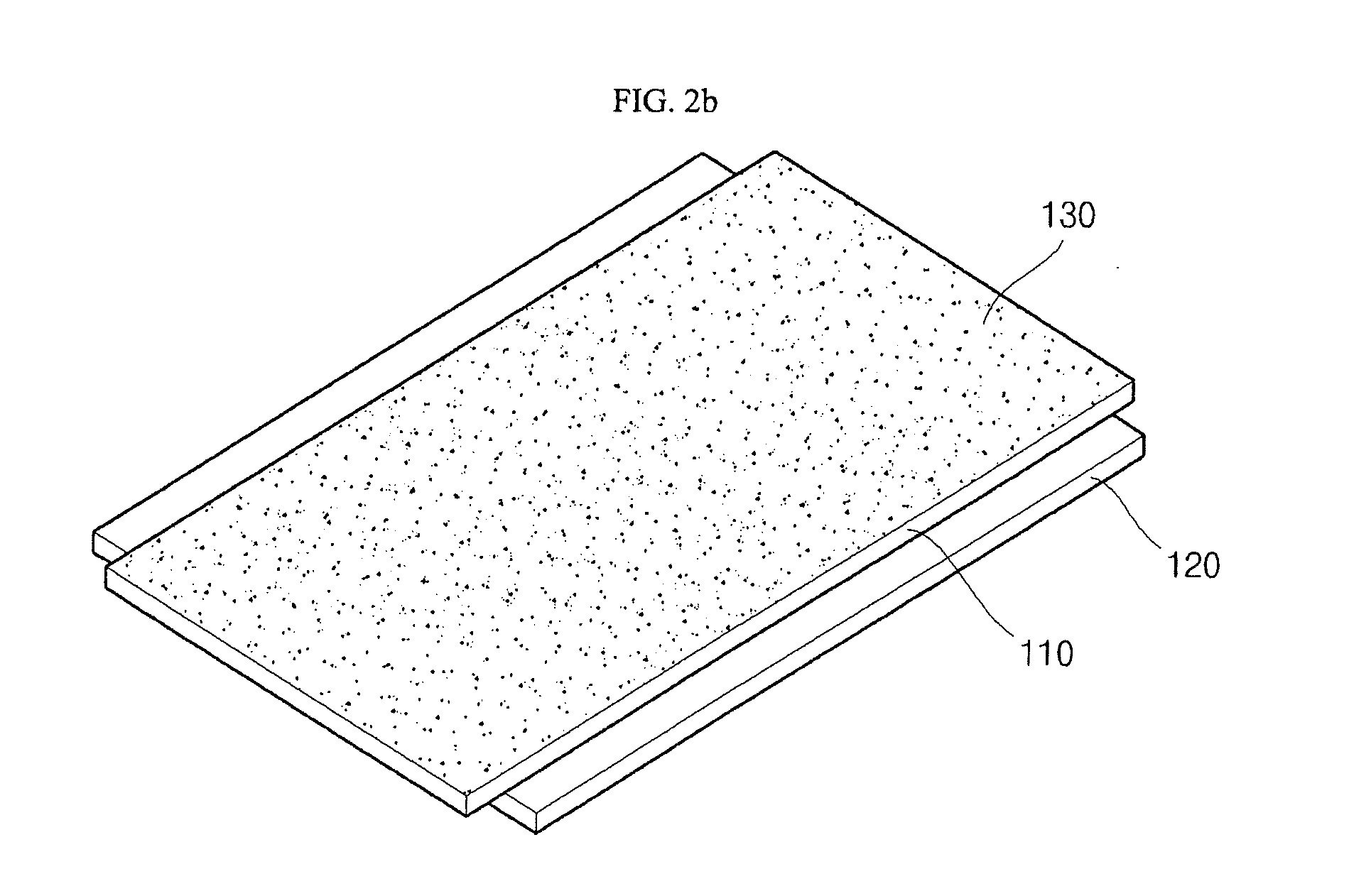
[0022]FIG. 1 is a flow chart illustrating a method of manufacturing an electromagnetic interference (EMI) shielding filter (i.e., an electromagnetic wave shield) for a plasma display panel in accordance with one embodiment of the present invention, and FIGS. 2a through 2d are perspective views illustrating a method of manufacturing an electromagnetic interference (EMI) shielding filter for a plasma display panel in accordance with one embodiment of the present invention.

[0023]Referring to FIG. 1, the method of manufacturing the plasma display device in accordance with one embodi...


PUM

PropertyMeasurementUnit
Temperatureaaaaaaaaaa
Lengthaaaaaaaaaa

Abstract

A method of manufacturing an electromagnetic wave shield for a plasma display panel having a first panel having an image-displaying surface, the method including coating the image-displaying surface of the first panel with a coating solution to form a hydrophobic layer; applying a conductive ink to the hydrophobic layer utilizing an ink-jet applicator to form a pattern of the conductive ink; and heating the conductive ink and the hydrophobic layer to form a conductive mesh pattern on the hydrophobic layer.

Description

CROSS-REFERENCE TO RELATED APPLICATION[0001]This application claims priority to and the benefit of U.S. Provisional Patent Application No. 61 / 142,057, filed Dec. 31, 2008, the entire content of which is incorporated herein by reference.BACKGROUND OF THE INVENTION[0002]1. Field of the Invention[0003]An aspect of the present invention relates to a method of manufacturing an electromagnetic interference (EMI) shielding filter for a plasma display panel and an EMI shielding filter for plasma display panel using the same.[0004]2. Description of the Related Art[0005]A plasma display device often includes a plasma display panel having a discharge cell defined by an address electrode, a scan electrode and a sustain electrode, and phosphors being applied to the discharge cell; and a drive unit for driving the plasma display panel. The plasma display device displays images through the generation of visible rays in response to excitation of phosphors by the action of ultraviolet rays generated...

Claims


Application Information

Patent Timeline
IPC IPC(8): H01J63/08H01J9/00
CPCH01J9/205H01J11/10H01J11/44H01J2211/446Y10T428/31645H05K9/0096
Inventor LIM, JAESEOKJIN, SANGYOUNGKIM, MINHYUNGYOON, HEEYOULJU, RIAPYO, YOUNGHAKPAEK, SEUNGHYUCKSEO, SANGCHUL
Owner SAMSUNG SDI CO LTD
Why Eureka
Try Eureka