
Circuit and Method for a High Speed Memory Cell
a memory cell and circuit technology, applied in the direction of information storage, static storage, digital storage, etc., can solve the problems of long read cycle time, reads of the memory cell to be destructive, and reads to be destructive, so as to improve the operation of the high-speed sense amplifier. , the effect of improving the operation of the sense amplifier
- Summary
- Abstract
- Description
- Claims
- Application Information
AI Technical Summary
Benefits of technology
Problems solved by technology
Method used
Image

Examples
Embodiment Construction
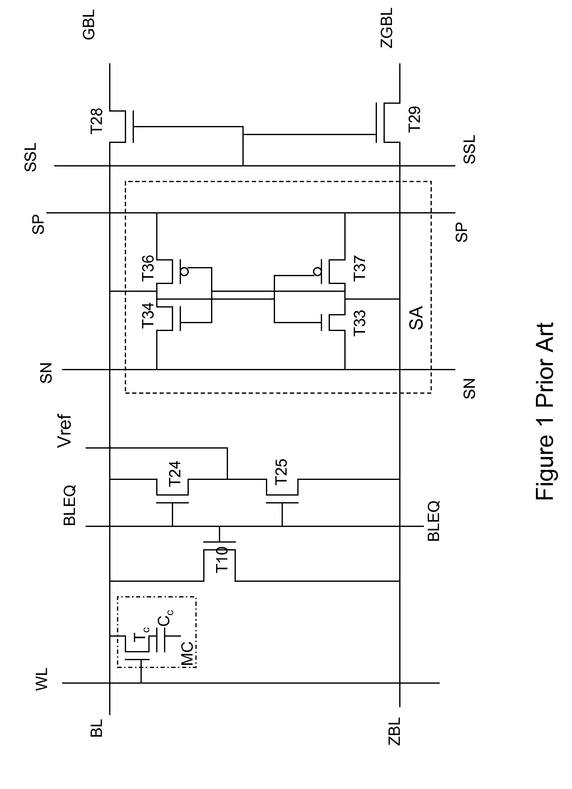
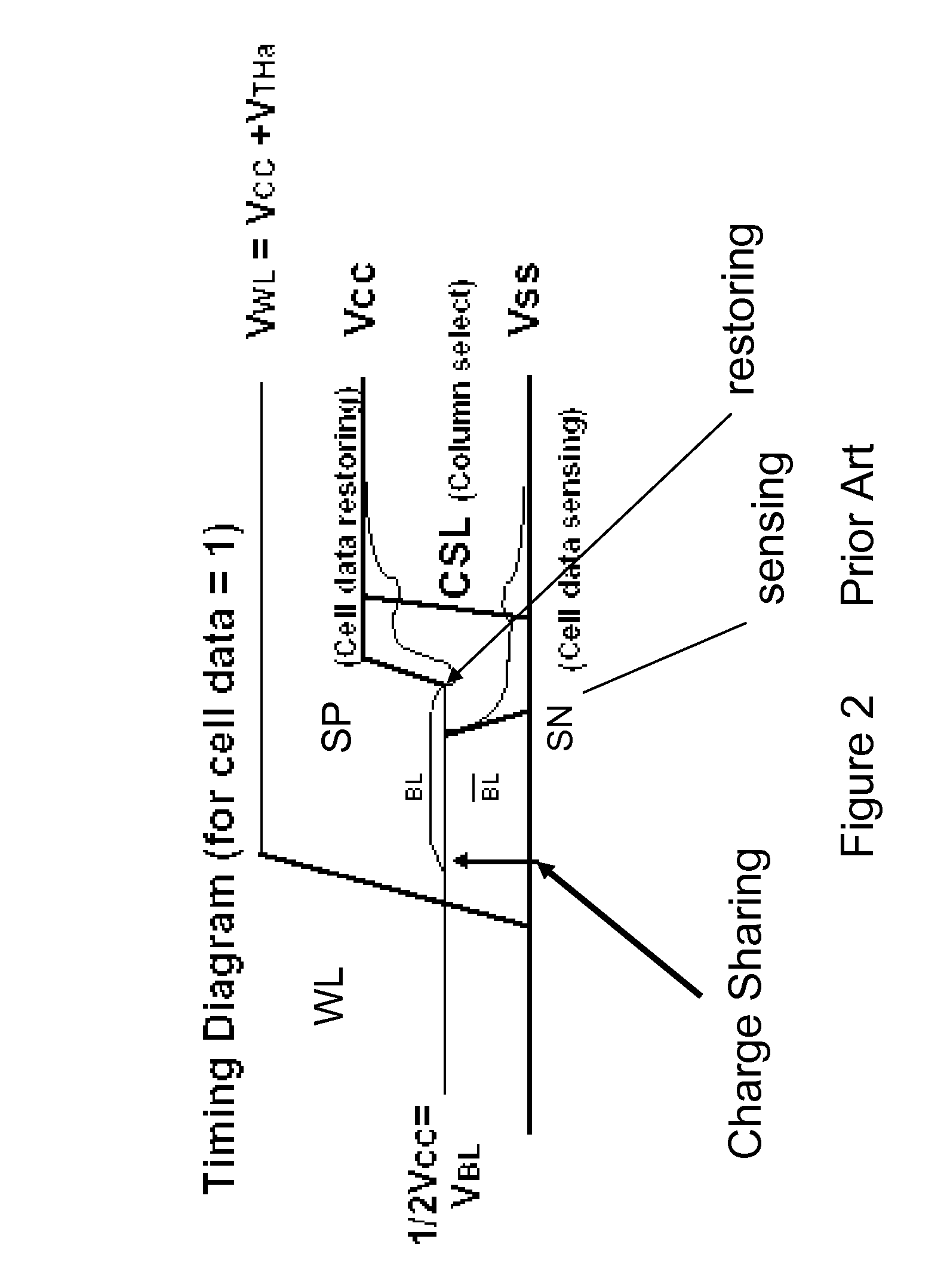
[0020]FIG. 1 depicts a small portion of a typical dynamic memory circuit of the prior art. Any read of a conventional dynamic memory cell such as the 1T1C cell MC in FIG. 1 is destructive, so the cell is always restored or rewritten at the end of the cycle. A “write” is simply a read cycle with write data impressed on the respective local bit line during the “restore” portion of the cycle. For a write, the read data is replaced or overwritten with the new write data and then written into the cell. Refresh cycles are also performed periodically to overcome loss of charge due to leakage.
[0021]In FIG. 1, memory cell MC is coupled at an intersection between a row or word line WL and a column or bit line BL. Although only one memory cell MC is depicted, another cell will be placed at the intersection of each of a plurality of word lines WL and the bit line BL. Similarly, a plurality of memory cells will also be placed at the intersections of each of a plurality of row lines WL (only one ...
PUM
 Abstract
Description
Claims
Application Information