Method for bonding two materials

a technology of bonding and materials, applied in metal working devices, manufacturing tools, semiconductor devices, etc., can solve the problems of incomplete bonding between the epitaxial layer and the conductive material, poor electrical and thermal conductivity, adverse influence on the quality of light-emitting diodes, etc., to avoid stress, improve manufacturing yield, and damage to materials

Inactive Publication Date: 2010-07-08
ADVANCED OPTOELECTRONICS TECH
View PDF8 Cites 19 Cited by
  • Summary
  • Abstract
  • Description
  • Claims
  • Application Information

AI Technical Summary

Benefits of technology

[0013]In the above-mentioned methods, the material of the high magnetic permeability metal layer is iron, cobalt, nickel or an alloy thereof, and the medium layer is a medium metal layer. The material of the medium layer is indium, tin, zinc, silver, or an alloy thereof. The bonding temperature (which, on average, is below 200 degrees Celsius) in the two methods for bonding two materials is less than the bonding temperature required by conventional methods so that the methods of the present invention are suitable for materials that cannot withstand high temperature, and the methods can therefore avoid stresses caused by thermal expansion or cooling shrinkage and resulting in the damage of materials. Compared to conventional methods, the methods of the present invention can improve the manufacturing yield.

Problems solved by technology

However, the substrate lattice matched to the epitaxial layer usually has poor electrical and thermal conductivity so that after the epitaxial process is performed, a conductive material is attached to the epitaxial layer as electrodes.
The bonding of the epitaxial layer and the conductive material is a heterogeneous bonding, which may have an adverse influence on the quality of the light emitting diodes.
However, the oscillation induced by the thermal ultrasonic energy may cause the interface between the epitaxial layer and the conductive material to have incomplete bonding due to frictional oscillation.
As a result, the manufacturing yield of light emitting diodes may be affected, and therefore a better method is needed.
However, the epitaxial layer and the conductive material may easily crack at a lower environmental temperature due to the cooling shrinkage thereof.
In addition, in the high voltage environment during bonding, electromagnetic field is created by accumulated electrical charges, causing high voltage difference across optoelectronic semiconductor devices and resulting in damage to the optoelectronic semiconductor devices.
Although the glass frit material can achieve firm bonding, bonded materials may suffer from cracking due to the cooling shrinkage thereof.
Therefore, the glass frit material is not suitable as the bonding material to bond the epitaxial layer and the conductive material.
For the bonding of an epitaxial layer and a conductive material, the crystal lattice of the epitaxial layer may be damaged by high temperatures (900° C.
), and the epitaxial layer may suffer from cracking due to the cooling shrinkage thereof.
Therefore, the method is not suitable for a light emitting diode process.
Although the bonding method is suitable for light emitting diodes, the epitaxial layer cannot avoid cracking caused by the shrinkage thereof when the epitaxial layer is cooled from a high temperature to a low temperature.
Moreover, an external force is required to remove the epitaxial layer from the substrate, to which the epitaxial layer is attached, and such a removal method may damage the epitaxial layer and lower the manufacturing yield of light emitting diodes.

Method used


Image

  • Method for bonding two materials
  • Method for bonding two materials
  • Method for bonding two materials

Examples


Embodiment Construction

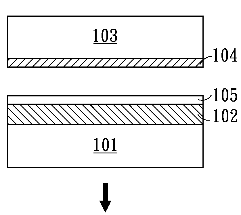
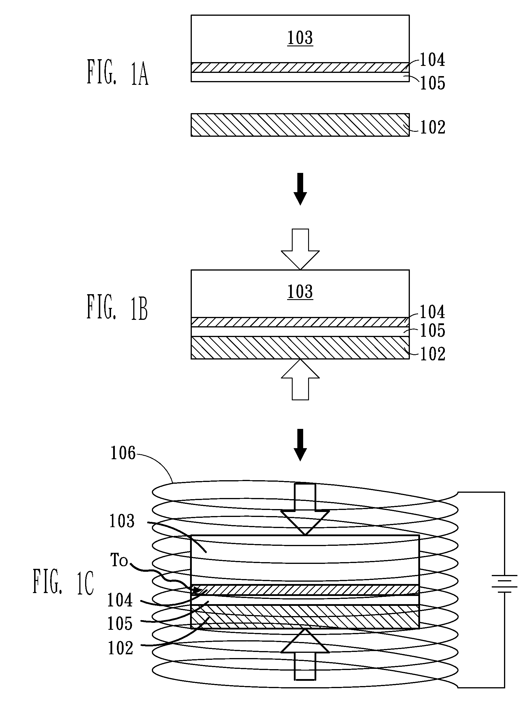
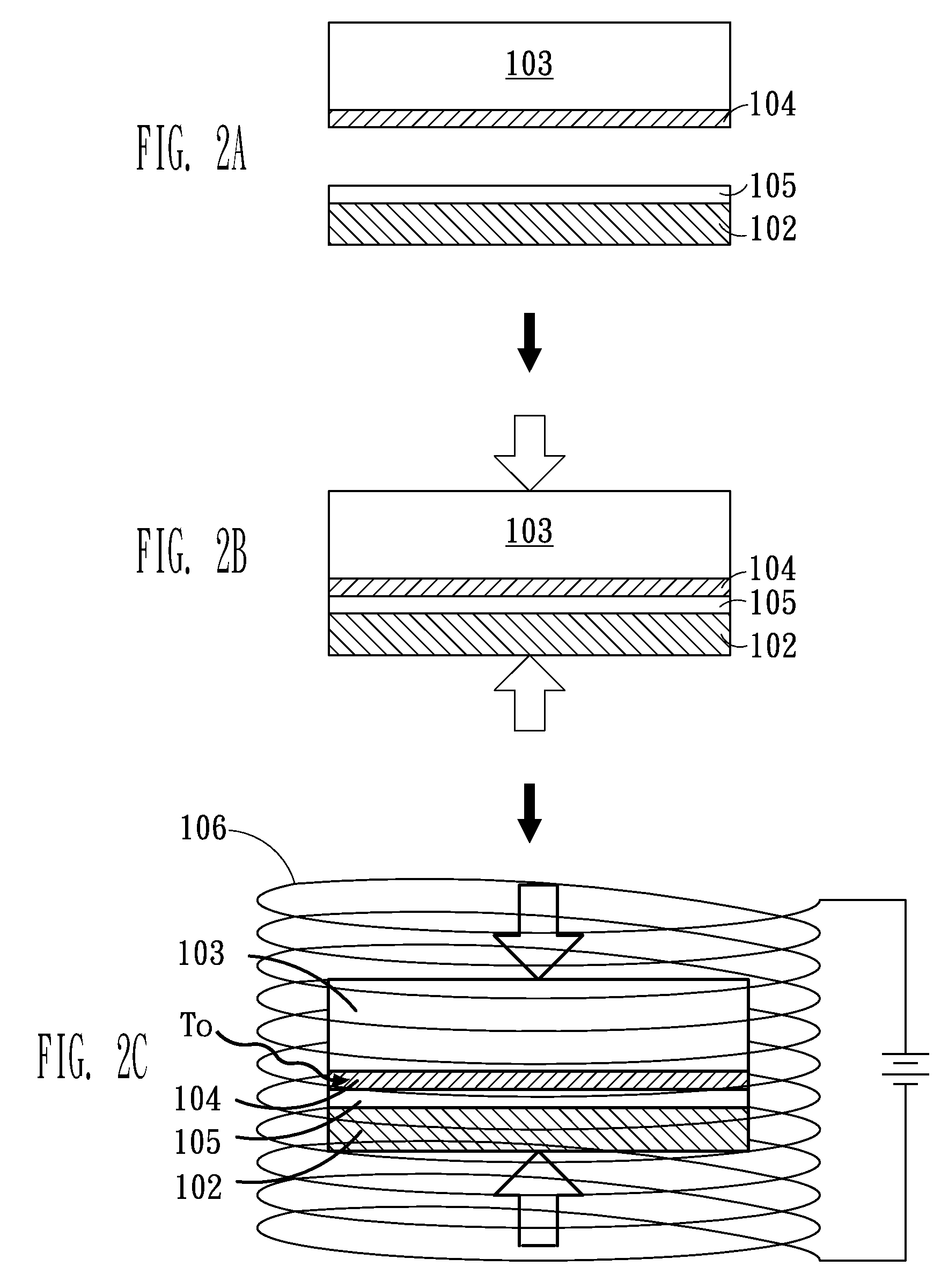
[0020]The present invention exemplarily demonstrates embodiments of a method for bonding two different semiconductor materials. In order to thoroughly understand the present invention, detailed descriptions of method steps and components are provided below. It should be noted that the implementations of the present invention are not limited to the specific details that are familiar to persons in the art related to semiconductor manufacturing processes, and such details are omitted to avoid unnecessary limitations to the present invention. On the other hand, components or method steps, which are well known, are not described in detail. A preferred embodiment of the present invention is described in detail below. However, in addition to the preferred detailed description, other embodiments can be broadly employed, and the scope of the present invention is not limited by any of the embodiments, but should be defined in accordance with the following claims and their equivalent.

[0021]The...


PUM

PropertyMeasurementUnit
temperatureaaaaaaaaaa
voltageaaaaaaaaaa
operating temperatureaaaaaaaaaa

Abstract

A method for bonding two materials uses radio frequency energy to swiftly induce heat in a high permeability material for heating a medium to the bonding temperature of the medium so as to bond the two materials with each other.

Description

BACKGROUND OF THE INVENTION[0001]1. Field of the Invention[0002]The present invention relates to a bonding method, and relates more particularly to a method for bonding two materials, which uses a radio frequency heating system to facilitate the bonding of the two materials.[0003]2. Description of the Related Art[0004]In a semiconductor method for manufacturing a light emitting diode, the epitaxial process, performed with other processes, uses a substrate, to which a GaN (gallium nitride) crystal can attach, for depositing an epitaxial layer on the substrate. The main considerations of the adoption of a substrate for the deposition process are the degree of the match of the lattice constants of the substrate and the epitaxial layer, and the match of the coefficients of thermal expansion of the substrate and the epitaxial layer. With matched lattice constants and coefficients of thermal expansion, the epitaxial layer is able to grow on the substrate. However, the substrate lattice ma...

Claims


Application Information

Patent Timeline
Patent Type & Authority Applications(United States)
IPC IPC(8): B23K31/02
CPCB23K13/01B23K2101/40H01L33/0079H01L21/187H01L33/0093
Inventor TU, PO MINHUANG, SHIH CHENGYEH, YING CHAOLIN, WEN YUWU, PENG YICHAN, SHIH HSIUNG
Owner ADVANCED OPTOELECTRONICS TECH
Why Eureka
Try Eureka