Isolation Structure for Stacked Dies

a technology of isolation structure and die, which is applied in the direction of semiconductor devices, semiconductor/solid-state device details, electrical apparatus, etc., can solve the problems of minimum size needed to make these components, physical limits of the density that can be achieved in two dimensions, and the requirement of more complex designs

Inactive Publication Date: 2010-07-08
TAIWAN SEMICON MFG CO LTD
View PDF98 Cites 57 Cited by
  • Summary
  • Abstract
  • Description
  • Claims
  • Application Information

AI Technical Summary

Benefits of technology

[0008]These and other problems are generally reduced, solved or circumvented, and technical advantages are g...

Problems solved by technology

Although dramatic improvement in lithography has resulted in considerable improvement in 2D integrated circuit (IC) formation, there are physical limits to the density that can be achieved in two dimensions.
One of these limits is the minimum size needed to make these components.
Also, when more devices are put into one chip, more complex designs are required.
The dielectric processes used on the circuit side of the subst...

Method used


Image

  • Isolation Structure for Stacked Dies
  • Isolation Structure for Stacked Dies
  • Isolation Structure for Stacked Dies

Examples


Embodiment Construction

[0017]The making and using of the presently preferred embodiments are discussed in detail below. It should be appreciated, however, that the present invention provides many applicable inventive concepts that can be embodied in a wide variety of specific contexts. The specific embodiments discussed are merely illustrative of specific ways to make and use the invention, and do not limit the scope of the invention.

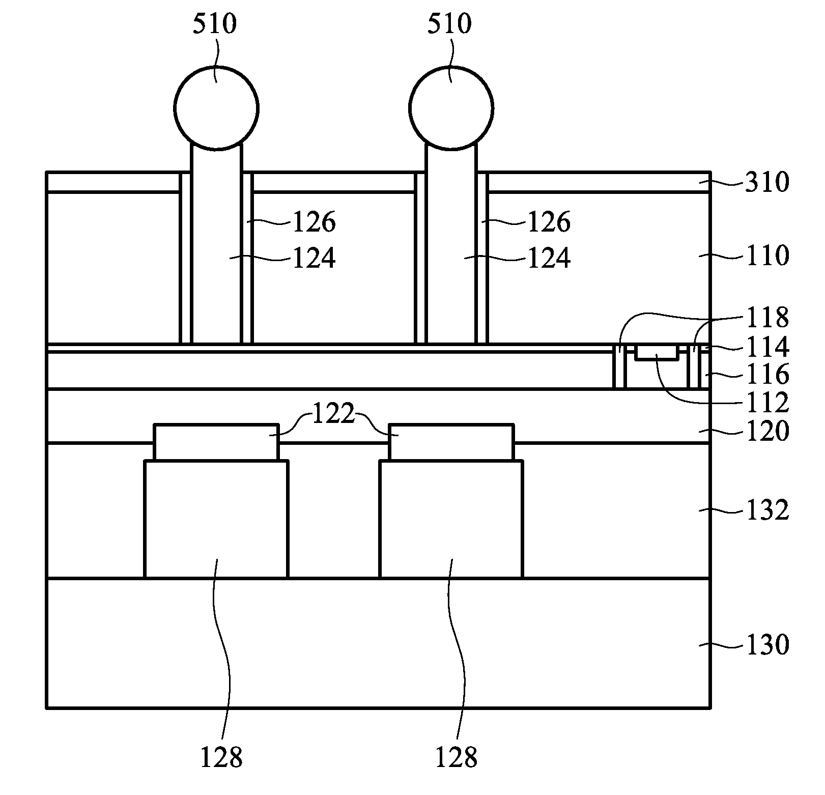
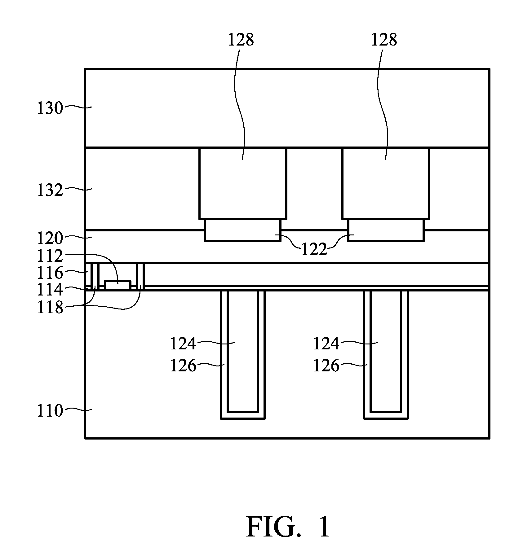
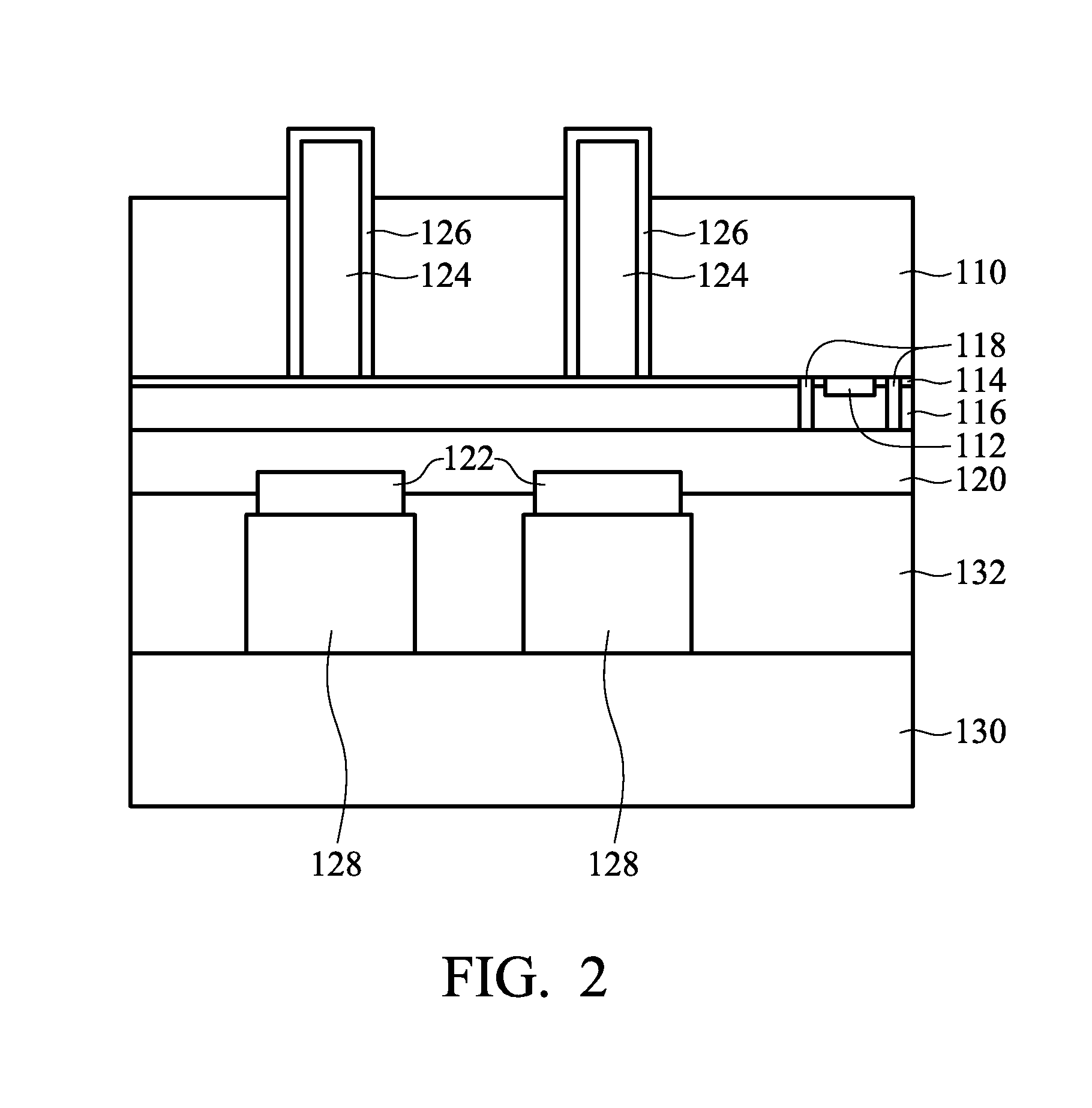
[0018]The intermediate stages of a method for forming a die having an isolation structure suitable for use in a three-dimensional integrated circuit or stacked die configuration are illustrated in FIGS. 1-5. Throughout the various views and illustrative embodiments of the present invention, like reference numbers are used to designate like elements.

[0019]Referring first to FIG. 1, a semiconductor substrate 110 having electrical circuitry 112 formed thereon is shown. The semiconductor substrate 110 may comprise, for example, bulk silicon, doped or undoped, or an active layer o...


PUM


Abstract

An isolation structure for stacked dies is provided. A through-silicon via is formed in a semiconductor substrate. A backside of the semiconductor substrate is thinned to expose the through-silicon via. An isolation film is formed over the backside of the semiconductor substrate and the exposed portion of the through-silicon via. The isolation film is thinned to re-expose the through-silicon via, and conductive elements are formed on the through-silicon via. The conductive element may be, for example, a solder ball or a conductive pad. The conductive pad may be formed by depositing a seed layer and an overlying mask layer. The conductive pad is formed on the exposed seed layer. Thereafter, the mask layer and the unused seed layer may be removed.

Description

TECHNICAL FIELD[0001]This invention relates generally to integrated circuits and, more particularly, to an isolation structure for stacked dies.BACKGROUND[0002]Since the invention of the integrated circuit, the semiconductor industry has experienced rapid growth due to continuous improvements in the integration density of various electronic components (e.g., transistors, diodes, resistors, capacitors, etc.). For the most part, this improvement in integration density has come from repeated reductions in minimum feature size, which allows more components to be integrated into a given area.[0003]These integration improvements are essentially two-dimensional (2D) in nature, in that the volume occupied by the integrated components is essentially on the surface of the semiconductor wafer. Although dramatic improvement in lithography has resulted in considerable improvement in 2D integrated circuit (IC) formation, there are physical limits to the density that can be achieved in two dimensi...

Claims


Application Information

Patent Timeline
IPC IPC(8): H01L23/48H01L21/34
CPCH01L21/6835H01L23/481H01L2924/12042H01L2924/15788H01L2224/0401H01L2924/01327H01L2924/014H01L24/11H01L24/13H01L24/14H01L2221/6834H01L2224/03912H01L2224/05009H01L2224/05558H01L2224/1147H01L2224/13009H01L2224/13025H01L2924/01013H01L2924/01015H01L2924/01022H01L2924/01029H01L2924/01047H01L2924/01073H01L2924/01074H01L2924/01075H01L2924/01078H01L2924/01079H01L2924/04953H01L2924/14H01L2924/19041H01L2924/19043H01L2924/00013H01L2924/01005H01L2924/01006H01L2924/01019H01L2924/01033H01L2224/13099H01L2924/00
Inventor CHANG, HUNG-PINHSU, KUO-CHINGCHEN, CHEN-SHIENCHIOU, WEN-CHIHYU, CHEN-HUA
Owner TAIWAN SEMICON MFG CO LTD
Why Eureka
Try Eureka