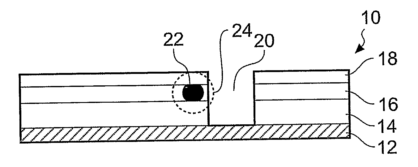
[0009]This provides an evanescent
optical field device with a lateral geometry, in that the waveguide and the groove are arranged side-by-side in the plane of the substrate, giving a horizontal configuration assuming the device is oriented with the substrate horizontal. This offers a range of advantages over the conventional vertical configuration of a surface window over the waveguide. For example, under the invention, the waveguide can have a curved path through the core and hence be smoothly brought into proximity with the groove. This gives an adiabatic change in the geometry and avoids the abrupt edge changes of a window that produce undesirable reflection effects. Also, the lateral configuration gives great flexibility to the relative arrangement of the waveguide and the groove. The waveguide can access the groove at multiple points, and it is straightforward to provide any amount of proximity. Further, the use of a groove instead of a surface window removes the need to use
acid etching, because the groove can be formed by a variety of other simpler and less hazardous techniques.
[0010]There is substantial flexibility available for manufacturing the device. The lateral geometry allows either the waveguide or the groove to be made first. In particular, the groove may be formed before the waveguiding channel is formed. This is different from conventional window arrangements where the window must be made after the waveguide, so that the intricate effort of making the waveguide is wasted if an error occurs in making the window. The present invention allows the simple step of making the groove to be performed first so that an already written waveguide is not wasted in the event of an error.
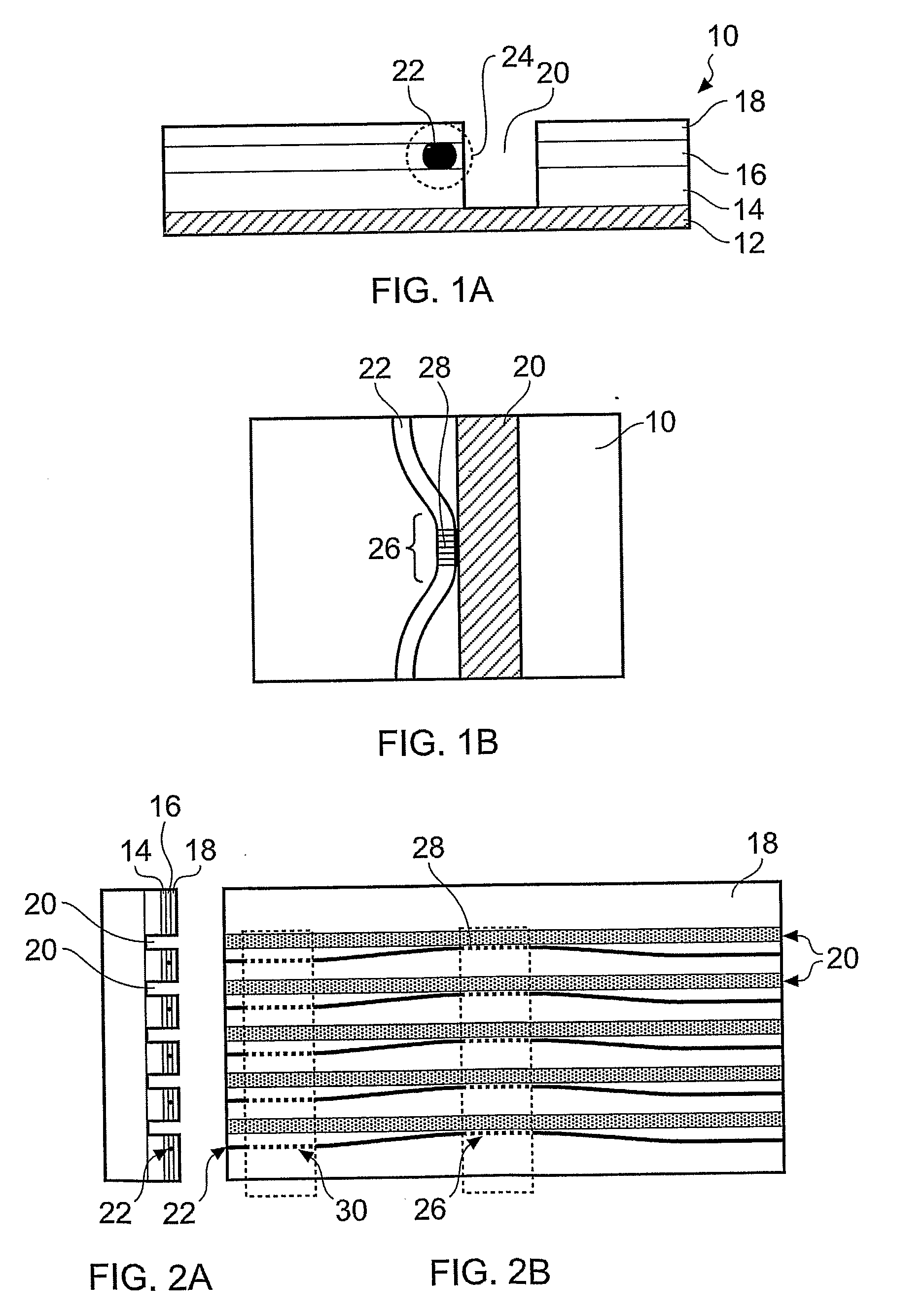
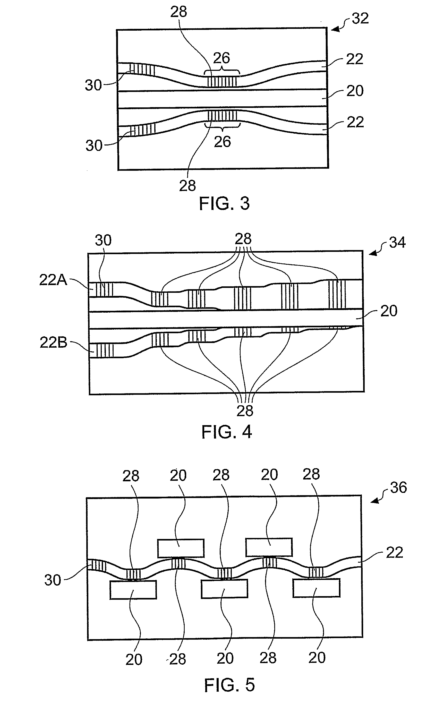
[0011]The method may further comprise forming a Bragg
grating in the part of the waveguiding channel
proximate to the groove. The inclusion of a
grating allows the device to perform a range of functions, such a
refractive index measurement of a sample material in the groove, or tuning of the grating by modification of an active material in the groove. The method is thus versatile in allowing many different devices to be fabricated in a simple manner.
[0012]For example, the core layer may be, photosensitive, and the waveguiding channel and any Bragg grating may be formed by exposing parts of the core layer to a spot of
ultraviolet light to produce a change in
refractive index. Further, the spot of
ultraviolet light may have a periodic intensity pattern of high and low intensity fringes.
Direct writing of a waveguide with a writing spot of
ultraviolet light is an attractively simple technique that allows complex waveguide configurations incorporating gratings to be created in a single fabrication step. Precise positioning of the waveguide is readily achievable, so that if the groove is formed first, using a low precision process, subsequent ultraviolet writing of the waveguide can provide the appropriate level of positional accuracy between the groove and the waveguide.
[0013]For example, if the groove is formed before the waveguiding channel is formed, the position of the spot of
ultraviolet light relative to the groove in the plane of the substrate may be tested during formation of the waveguiding channel by measuring the amount of light transmitted from the spot into the groove. This is a simple technique by which the separation between the waveguide and the groove can be accurately controlled during waveguide formation.
[0023]In alternative embodiments, the optical waveguide device may be a refractive index sensor, and the method may further comprise: forming a second groove in the substrate, filling the groove with
liquid crystal and providing the substrate with electrodes by which an
electric field can be applied across the
liquid crystal; forming a second waveguiding channel arranged to collect light reflected from or transmitted by the Bragg grating in the said waveguiding channel, the second waveguiding channel having a portion sufficiently
proximate to the second groove in the plane of the substrate for an evanescent field of light propagating in the second waveguide to extend laterally into the second groove; and forming a second Bragg grating in the proximate part of the second waveguiding channel such that application of an
electric field across the
liquid crystal can modify the Bragg
wavelength of the second Bragg grating. This gives a device in which measuring the light from the second grating while that grating is tuned in
wavelength allows a
spectral analysis to be performed of the light from the first grating that is measuring the refractive index of any material in the groove.

