Photodetector/imaging device with avalanche gain

a photodetector and imaging device technology, applied in the direction of x/gamma/cosmic radiation measurement, radioation controlled devices, instruments, etc., can solve the problems of discharge generating an electric current that rises uncontrollably, without bounds, and using the avalanche properties of acps in solid-state devices for very high sensitivity

Active Publication Date: 2010-07-22
THE RES FOUND OF STATE UNIV OF NEW YORK +1
View PDF12 Cites 17 Cited by
  • Summary
  • Abstract
  • Description
  • Claims
  • Application Information

AI Technical Summary

Problems solved by technology

The key limitation to utilizing the avalanche properties of ACPs in solid-state devices for very high sensitivity applications such as medical imaging has to do with the high electric fields required to precipitate hole and electron avalanche.
At the high electric fields required for avalanche multiplication, these electrical discharges produce an electric current that rises uncontrollably.
This effect, referred to as incipient breakdown, has the unfortunate consequence of irreversibly altering the structure of the photoconductive material of the ACP.
These vacuum tube devices, which are based on a-Se, derive their gain solely from the multiplication of a single charge carrier type (holes), as they are unable to support the higher electric fields at which the second charge carrier type (electrons) avalanches.
This chain reaction can rapidly grow without bounds and eventually causes the electric field inside the ACP to collapse.
Although the above-references show solid-state photodetector / imaging devices employing amorphous selenium that take advantage of avalanche multiplication, to-date none of these solid-state photodetector / imaging devices have been commercialized, primarily because of the limitation associated with incipient breakdown at high electric fields (i.e. fields greater than 10 V / um in a-Se).
Furthermore, these solid-state photodetector / imaging devices only take advantage of avalanche multiplication of a single type of charge carrier (holes).
As mentioned above, the need to apply a higher electric field further compounds the incipient breakdown problem since the amount of energy stored across the photoconductor grows quadratically as a function of the bias potential.

Method used


Image

  • Photodetector/imaging device with avalanche gain
  • Photodetector/imaging device with avalanche gain
  • Photodetector/imaging device with avalanche gain

Examples


Embodiment Construction

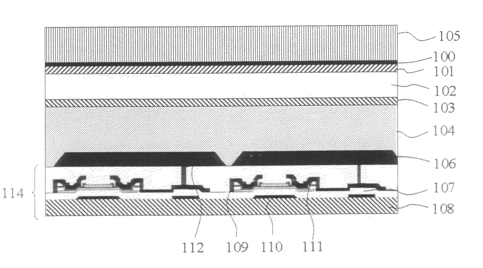
[0031]In the following, a photodetector / imaging device with avalanche gain is disclosed that avoids the undesirable effects associated with incipient breakdown allowing the photodetector / imaging device to be subjected to high electric fields sufficient to take advantage of avalanche multiplication of both types of charge carriers (holes and electrons). In one form, the photodetector / imaging device comprises a layer of photoconductive material for receiving incident electromagnetic radiation and for converting the electromagnetic radiation into electrical charges. The layer of photoconductive material is capable of avalanche multiplication when an electric field of sufficient magnitude is applied thereacross. At least one interface layer is provided for coupling electric charge to or from the layer of photoconductive material. A readout layer detects the electrical charge.

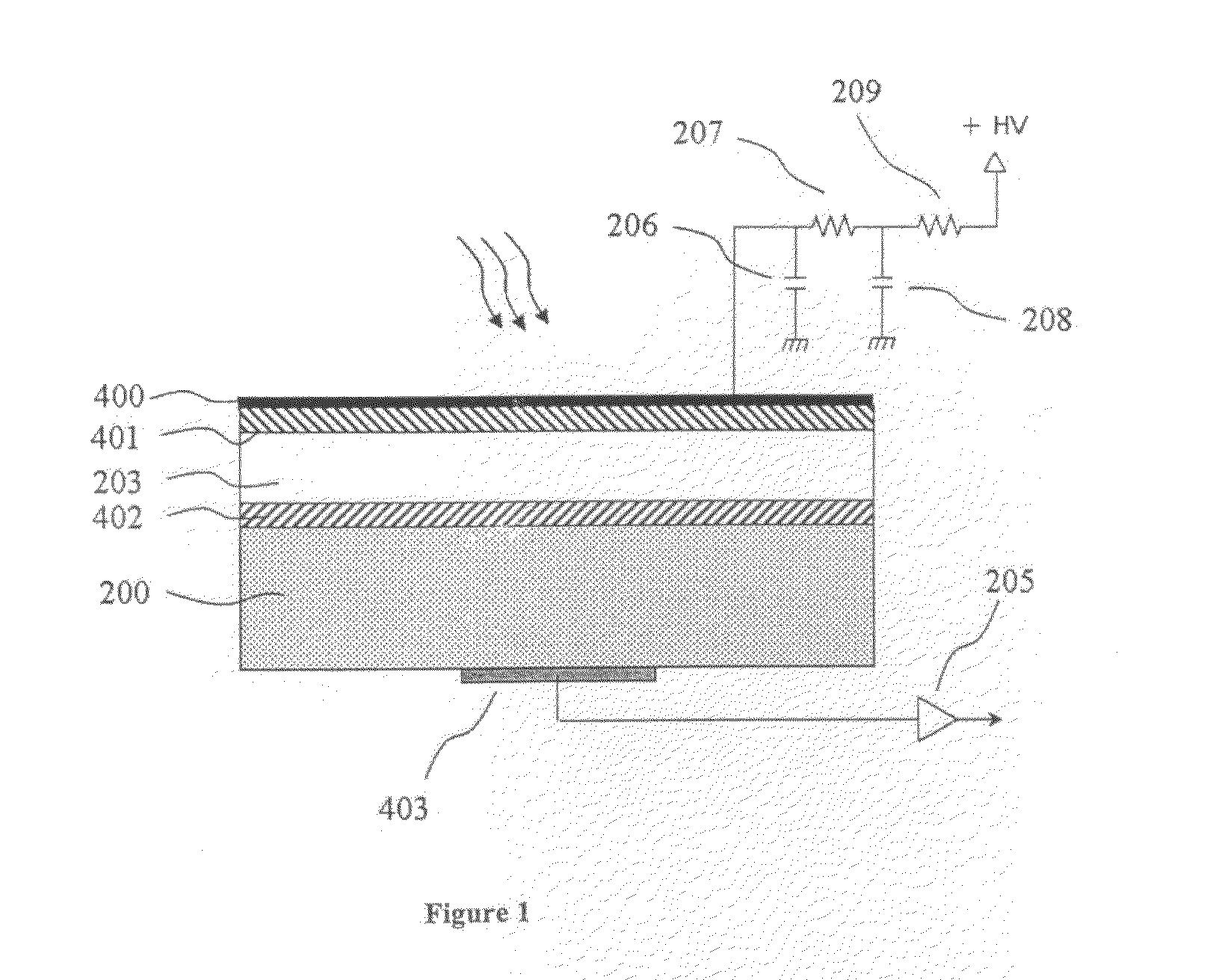
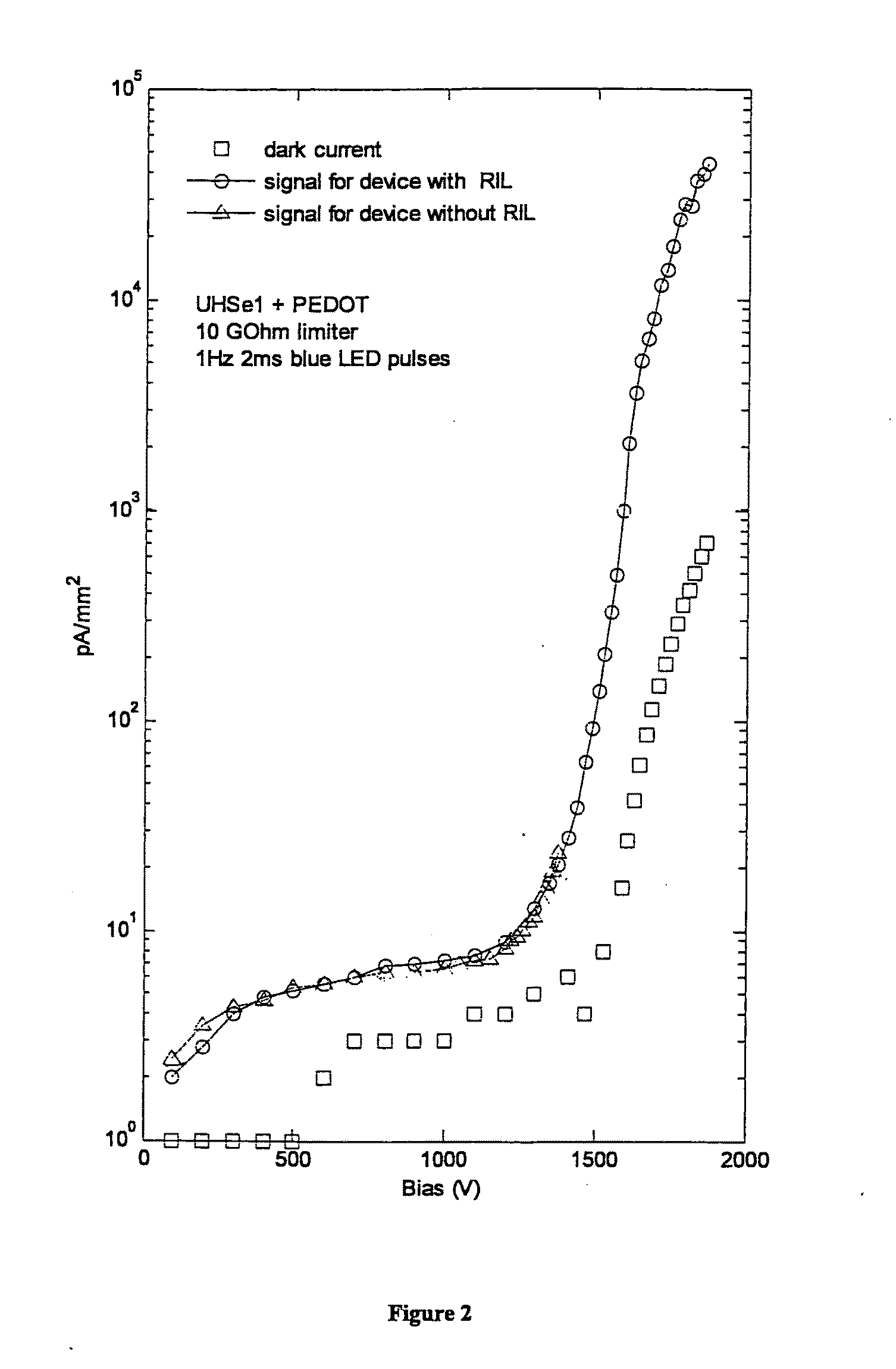
[0032]For proof of concept, an experimental photodetector device with avalanche gain was developed as shown in FI...


PUM


Abstract

A photodetector / imaging device comprises a layer of photoconductive material converting incident electromagnetic radiation into electrical charges, the layer of photoconductive material being capable of avalanche multiplication when an electric field of sufficient magnitude is applied thereacross; a readout layer detecting the electrical charge; and at least one interface layer between the layer of photoconductive material and the readout layer, the interface layer coupling electrical charge to or from the layer of photoconductive material and being configured to inhibit uncontrolled rises in current in the photoconductive material during avalanche multiplication.

Description

CROSS-REFERENCE TO RELATED APPLICATION[0001]This application claims the benefit of U.S. Provisional Application No. 61 / 129,389 to Wronski et al. filed on Jun. 23, 2008 entitled “Photodetector / Imaging Device with Avalanche Gain”, the contents of which are incorporated herein by reference.FIELD OF THE INVENTION[0002]The present invention relates generally to photon detection and imaging devices and in particular, to a photodetector / imaging device with avalanche gain.BACKGROUND OF THE INVENTION[0003]Chalcogenide glasses belong to a class of materials that exhibit a number of interesting electrical and optical properties. Amorphous selenium (a-Se), for instance, is a particularly prominent type of chalcogenide glass. It has photonconductive properties and has been used in a variety of devices including for example, photocopiers, medical imaging systems and high-definition television broadcasting cameras.[0004]Photoconductors are materials that are sensitive to visible light and other ty...

Claims


Application Information

Patent Timeline
Patent Type & Authority Applications(United States)
IPC IPC(8): H01L31/09H01L31/112H01L31/0352H01L31/107G01T1/208H01L27/148H01L27/146
CPCH01L27/14634H01L31/107H01L27/14665
Inventor WRONSKI, MATTHEW M.DECRESCENZO, GIOVANNIREZNIK, ALLAZHAO, WEISEGUI, JENNIFER ANNROWLANDS, JOHN A.
Owner THE RES FOUND OF STATE UNIV OF NEW YORK
Why Eureka
Try Eureka