Organic el display panel and manufacturing method thereof

a technology of organic el and display panels, which is applied in the direction of thermoelectric device junction materials, electrical apparatus, and semiconductor devices. it can solve the problems of non-uniform organic luminescent layer thickness, non-uniform thickness, and reduce the luminescence efficiency and, therefore, the lifetime of the organic el display panel. achieve the effect of high wettability and flat surfa

Active Publication Date: 2010-07-22
JOLED INC
View PDF15 Cites 72 Cited by
  • Summary
  • Abstract
  • Description
  • Claims
  • Application Information

AI Technical Summary

Benefits of technology

[0044]The present invention can provide an organic EL display panel with uniform thick organic layers because coating regions have high wettability and flat surface.

Problems solved by technology

Nevertheless, organic EL display panels manufactured with this method have had the disadvantage of non-uniform organic luminescent layer thickness because discrete organic luminescent layers are formed in regions defined by banks.
Namely, non-uniform thickness is caused by the surface tension of the applied ink, which pulls more liquid to the edges of the banks.
Non-uniformity in organic luminescent layer thickness reduces the luminescence efficiency and, accordingly, lifetime of an organic EL display panel.

Method used


Image

  • Organic el display panel and manufacturing method thereof
  • Organic el display panel and manufacturing method thereof
  • Organic el display panel and manufacturing method thereof

Examples


embodiment 1

[0167]In Embodiment 1, a top emission organic EL display panel will be described. Note that the organic EL display panel of Embodiment 1 is an active matrix display panel.

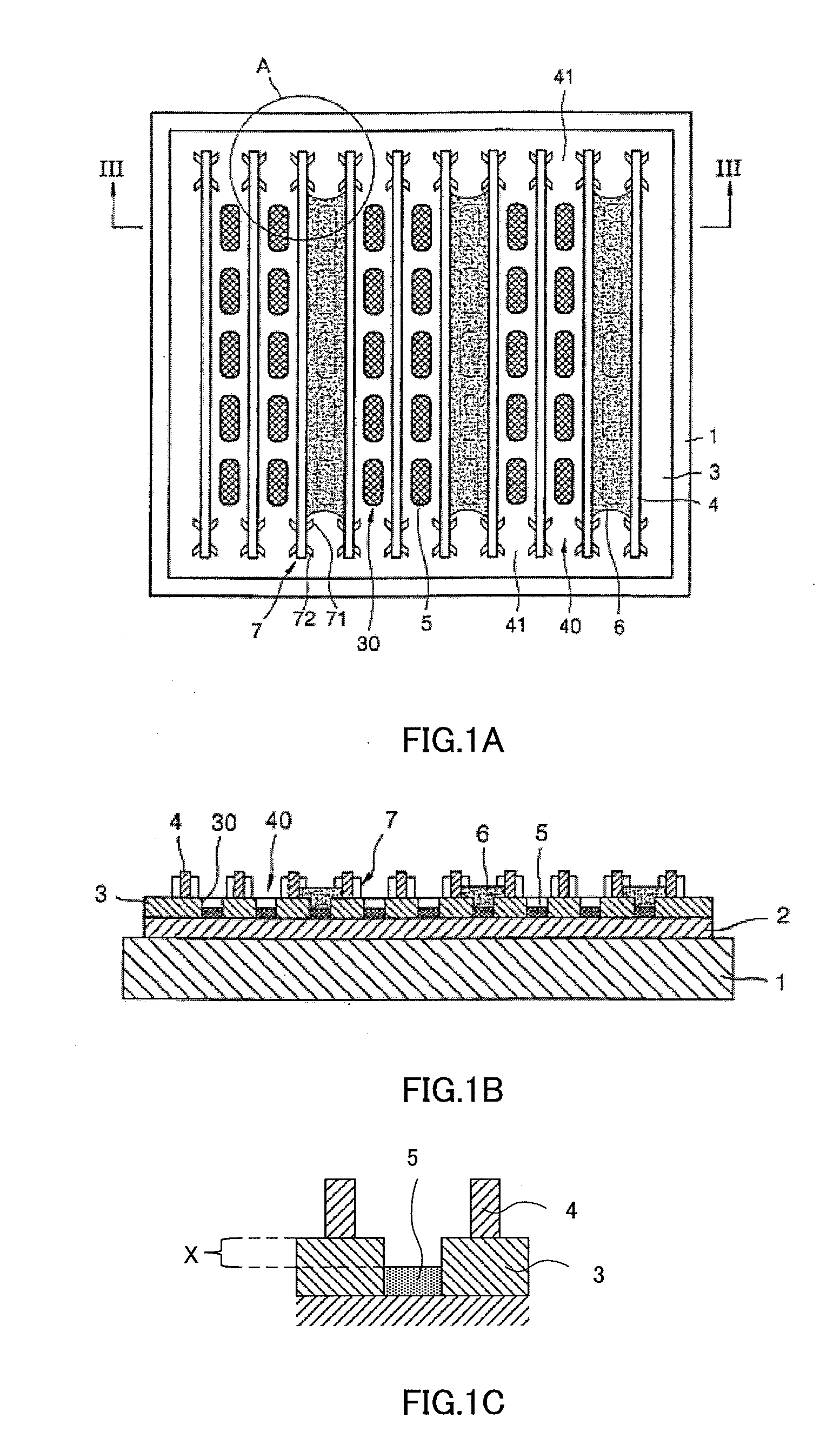
[0168]FIG. 6A is a plan view showing an active matrix organic EL display panel of Embodiment 1, where illustrations of a counter electrode and organic luminescent layers are omitted. FIG. 6B is a perspective view showing the organic EL display panel of FIG. 6A.

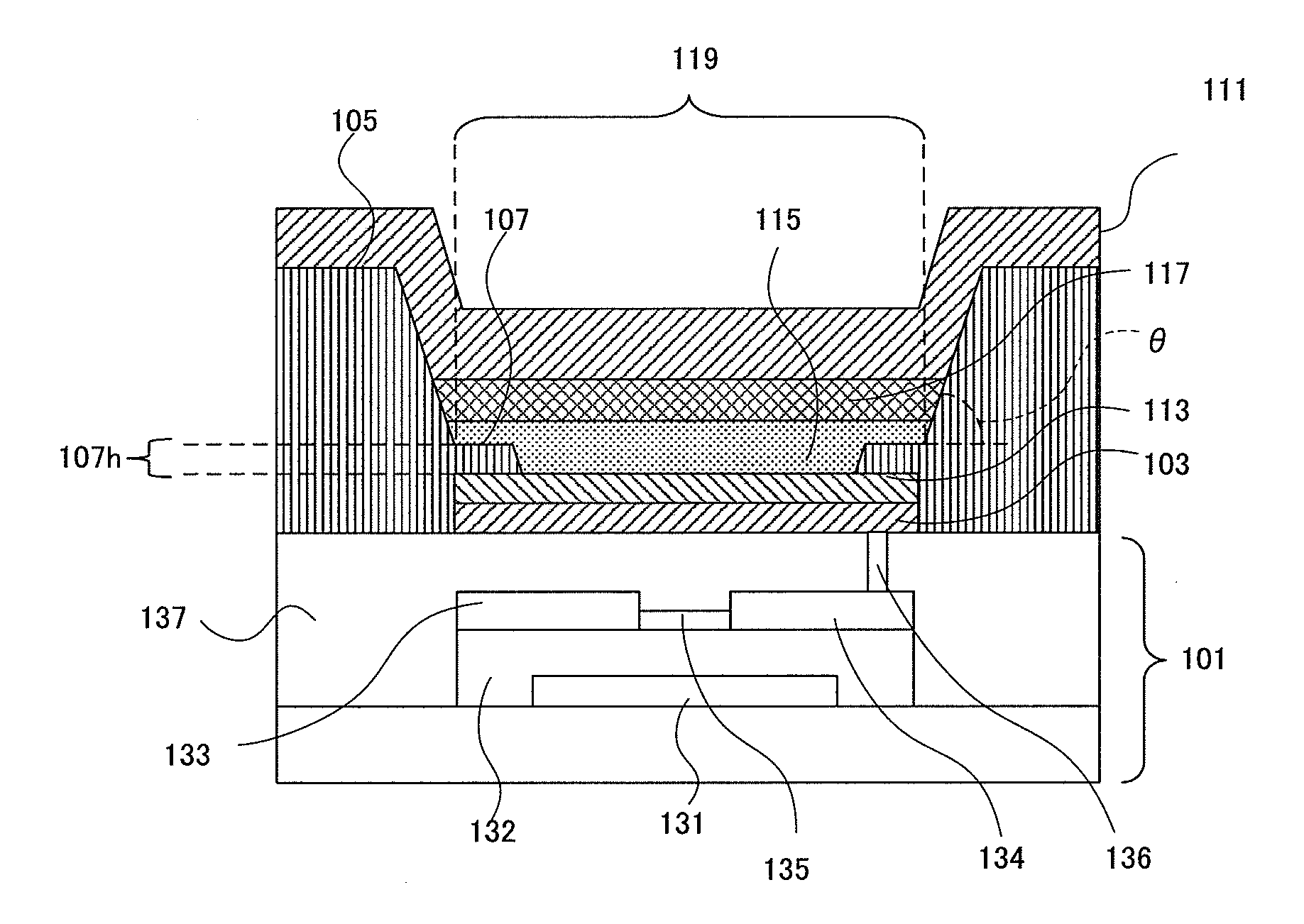
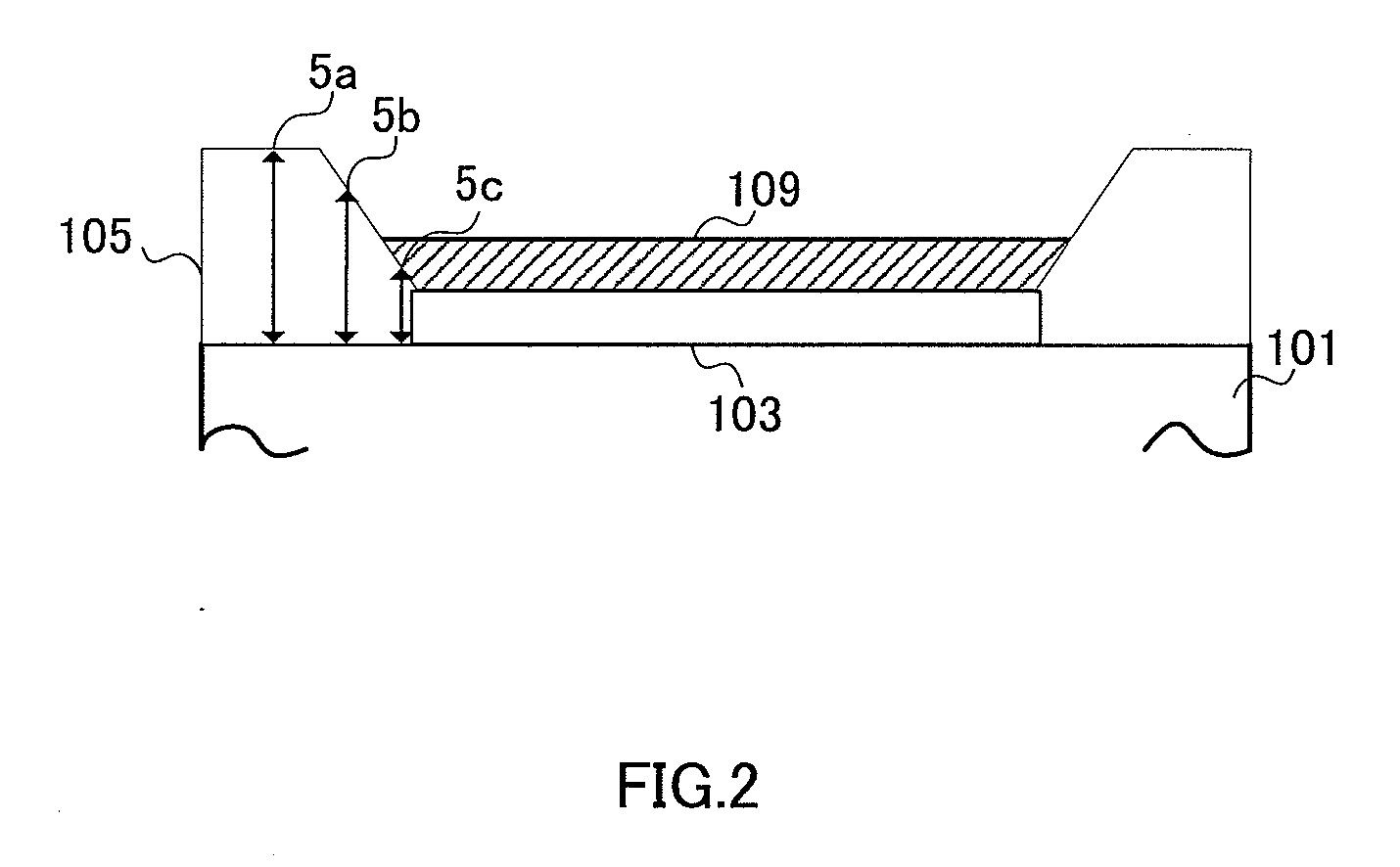
[0169]As shown in FIGS. 6A and 6B, in the organic EL display panel of Embodiment 1, multiple linear banks (first bank) 105 are disposed on substrate 101. First bank 105 defines coating regions 119, which are classified into three types: coating region 119R emitting red light; coating region 119G emitting green light; and coating region 119B emitting blue light. These three different coating regions are alternately arranged. Moreover, second bank 107 which is shorter in height than first bank 105 is disposed on substrate 101. Second bank 107 defines multiple p...

embodiment 2

[0181]In Embodiment 1, an example where a hole injection layer made of transition metal oxide is employed has been described. In Embodiment 2, an example where a PEDOT-PSS-containing hole injection layer is employed will be described.

[0182]An organic EL display panel of Embodiment 2 is identical to the organic EL display panel of Embodiment 1 except that 1) the hole injection material is PEDOT-PSS and that 2) the positional relationship between second bank and hole injection layer is different. Accordingly, the same members are given the same reference numerals and descriptions thereof are not provided.

[0183]FIG. 6A is a plan view showing an active matrix organic EL display panel of Embodiment 2, where illustrations of a counter electrode and organic luminescent layers are omitted. FIG. 6B is a perspective view showing the organic EL display panel of FIG. 6A.

[0184]FIG. 8A is an A-A line sectional view of an organic EL device contained in the organic EL display panel of Embodiment 2....

embodiment 3

[0220]In Embodiments 1 and 2, examples where longitudinal ends of coating regions are not defined have been described. In this embodiment, an example where longitudinal ends of coating regions are also defined by first bank is described. Moreover, Embodiments 1 and 3 provided descriptions of an embodiment where a second bank is disposed between a pixel region and a first bank (see FIGS. 6A and 6B), Embodiment 3 provides descriptions of an embodiment where a second bank is not disposed between a pixel region and a first bank.

[0221]An organic EL display panel of this Embodiment is identical to that of Embodiment 1 except that the former includes first bank 105′ for defining an end of a coating region and that the former does not include second bank 107 between pixel region 120 and first bank 105. Accordingly, the same members are given the same reference numerals and descriptions thereof are not provided.

[0222]FIG. 11A is a plan view showing an active matrix organic EL display panel o...


PUM


Abstract

Disclosed is an organic EL display panel which includes: a substrate; a linear first bank which is disposed over the substrate and defines a linear region; a second bank which defines two or more pixel regions arranged in the linear region; a pixel electrode disposed in the pixel region; a linear organic layer which is formed by coating method in the linear region over the pixel electrode and second bank; and a counter electrode over the organic layer, wherein the first bank is larger in height than the second bank, the first and second banks are made of resin, anisole contact angle at the top of the first bank is 30-60°, and anisole contact angle at the top of the second bank is 5-30°.

Description

TECHNICAL FIELD[0001]The present invention relates to an organic EL display panel and a manufacturing method of the same.BACKGROUND ART[0002]An organic EL display panel refers to a display panel which includes light-emitting devices exploiting electroluminescence (EL) of organic compounds. Specifically, the organic EL display panel has EL devices each including a pixel electrode, an organic luminescent layer disposed over the pixel electrode, and a counter electrode disposed over the organic luminescent layer. Organic EL materials used for the organic luminescent layer can be broadly classified into two types: combinations of low-molecular weight compounds (combinations of host and dopant materials); and organic polymer compounds. Examples of organic polymer compounds include polyphenylenevinylene (abbreviated as “PPV”) and its derivatives. An organic EL display panel that utilizes organic polymer compounds can be driven at relatively low voltage and consumes less power, lending its...

Claims


Application Information

Patent Timeline
Patent Type & Authority Applications(United States)
IPC IPC(8): H01L51/52H01L51/56
CPCH01L27/3246H01L51/0005H01L27/3283H10K59/122H10K59/173H10K71/135H10K71/00
Inventor NAKATANI, SHUHEIYOSHIDA, HIDEHIROTAKAGI, KIYOHIKO
Owner JOLED INC
Why Eureka
Try Eureka