
Organic electroluminescent element, display, and electronic apparatus

a technology of electroluminescent elements and electronic devices, applied in the direction of solid-state devices, semiconductor devices, thermoelectric devices, etc., can solve problems such as deterioration of lifetime characteristics, and achieve the effect of preventing the occurrence of dark and bright spots and satisfactory lifetime characteristics

Inactive Publication Date: 2010-07-22
JOLED INC
View PDF4 Cites 7 Cited by
  • Summary
  • Abstract
  • Description
  • Claims
  • Application Information

AI Technical Summary

Benefits of technology

[0006]Meanwhile, in an organic electroluminescent element, an organic material constituting an organic luminescent functional layer is readily degraded by reaction with water and oxygen. Thus, covering the entirety of the organic electroluminescent element with a protective film composed of an inorganic material such as silicon nitride prevents the infiltration of water and oxygen. In such a structure, however, a stress is readily generated between the protective film and the organic electroluminescent element. This causes a deterioration in lifetime characteristics due to the detachment of the organic electroluminescent element from the negative electrode and the occurrence of failure, such as dark and bright sports.
[0007]It is desirable to provide a highly reliable organic electroluminescent element having satisfactory lifetime characteristics without the occurrence of dark or bright sports and to provide a display and an electronic apparatus each including the organic electroluminescent element.
[0009]In the organic electroluminescent element having such a structure, despite the arrangement of the transition-metal-complex layer having low electron mobility between the electron-transport layer and the negative electrode, the lifetime characteristics are satisfactory, and the occurrence of dark and bright spots are prevented, as compared with an element that does not include the transition-metal-complex layer.

Problems solved by technology

This causes a deterioration in lifetime characteristics due to the detachment of the organic electroluminescent element from the negative electrode and the occurrence of failure, such as dark and bright sports.

Method used


Image

  • Organic electroluminescent element, display, and electronic apparatus
  • Organic electroluminescent element, display, and electronic apparatus
  • Organic electroluminescent element, display, and electronic apparatus

Examples


examples

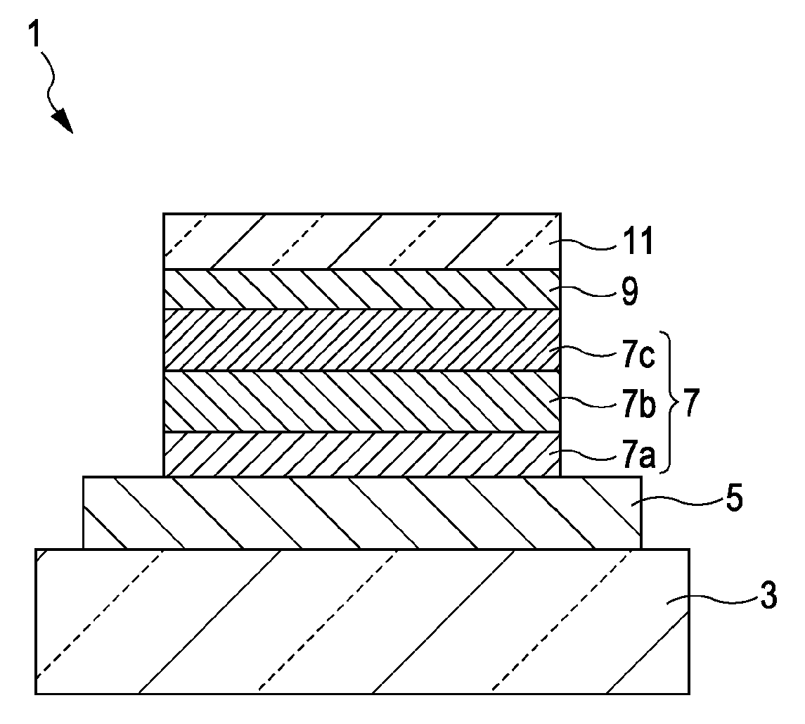
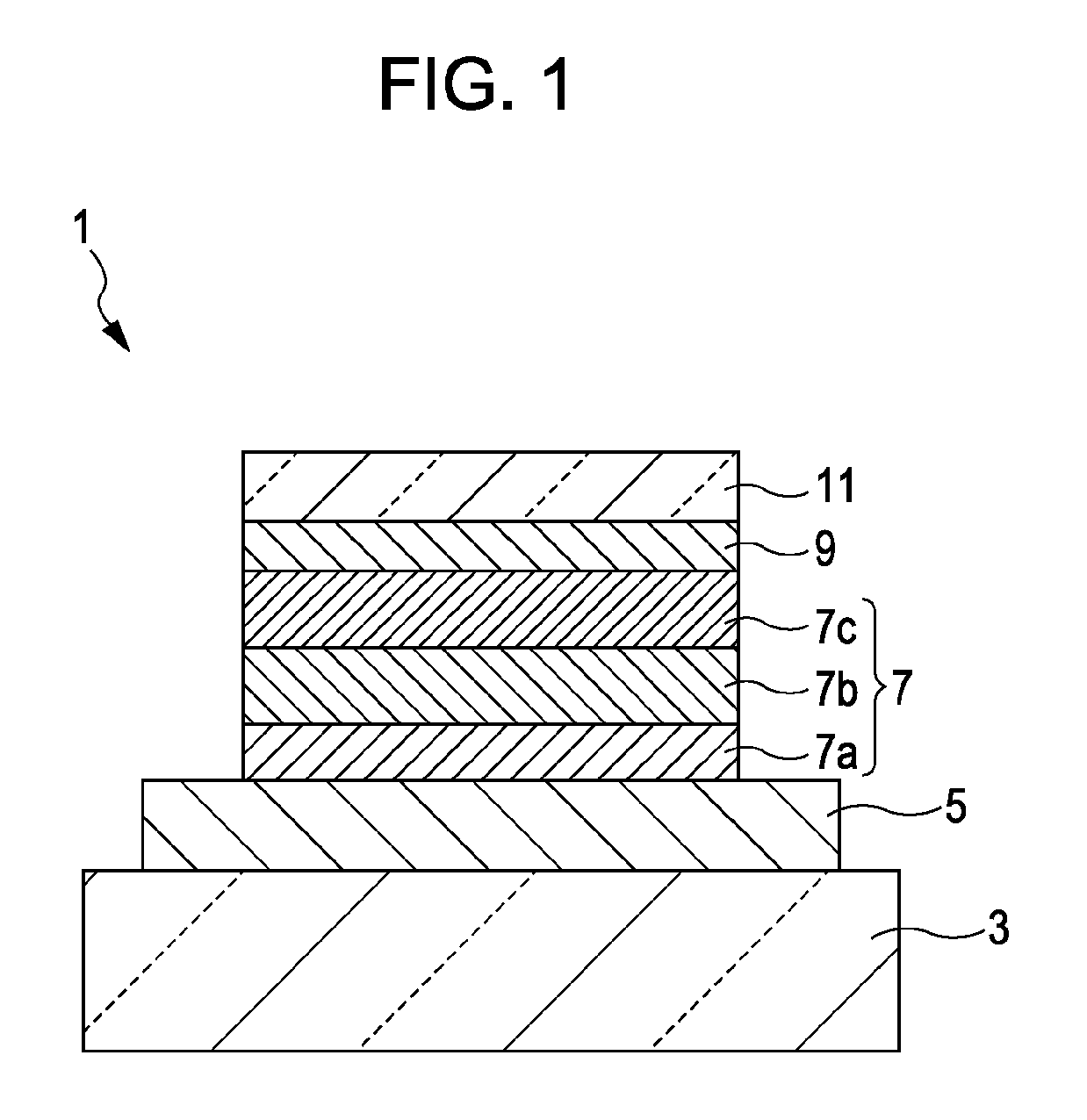
[0072]Procedures for making organic electroluminescent elements according to examples and comparative examples of the present invention will be described with reference to FIG. 1, and then evaluation results thereof will be described.

examples 8 to 14

[0082]The procedure was performed up to the formation of the luminous sublayer 7b as in Examples 1 to 7. The 15-nm-thick electron-transport sublayer 7c composed of compound (N-10) was formed. The transition-metal-complex layer 9 composed of compound (A-3) was formed so as to have a thickness of 0.1 nm to 25 nm. The negative electrode 11 in which a 12-nm-thick MgAg film was stacked on a 1-nm-thick lithium fluoride (LiF) film was formed.

[0083]Like Examples 1 to 7, a protective film was formed, and a glass substrate was bonded, thereby affording the top-emission organic electroluminescent element 1.

[0084]For each of the organic electroluminescent elements produced in Examples 8 to 14, a current efficiency (cd / A) was measured during driving at a current density of 10 mA / cm2. A load was driven at a constant current, a temperature of 50° C., a duty of 25%, and a current density of 50 mA / cm2. The time taken to reduce initial luminance 1 to 0.5 was measured as lifetime (hr).

[0085]Table 2 sh...


PUM


Abstract

An organic electroluminescent element includes an electron-transport layer composed of a heterocyclic compound, a negative electrode composed of a metal material, and a transition-metal-complex layer arranged between the electron-transport layer and the negative electrode.

Description

BACKGROUND OF THE INVENTION[0001]1. Field of the Invention[0002]The present invention relates to an organic electroluminescent element, a display, and an electronic apparatus, and in particular, to an organic electroluminescent element suitable for a structure in which light emerges from a negative electrode side and relates to a display and an electronic apparatus each including the organic electroluminescent element.[0003]2. Description of the Related Art[0004]Organic electroluminescent elements (organic EL elements) utilizing electroluminescence of organic materials each include an organic luminescent functional layer having a luminous sublayer provided between a positive electrode and a negative electrode and have been receiving attention as luminous elements capable of achieving high-luminance light emission at low-voltage DC drive. In organic electroluminescent elements, various layer structures have been studied in order to improve luminous properties and lifetime characteris...

Claims


Application Information

Patent Timeline
IPC IPC(8): H01L51/54
CPCH01L51/0072H01L51/0081H01L51/0083H01L51/0085H01L51/5092H01L51/0091H01L51/0092H01L51/50H01L51/5048H01L51/0089H10K85/331H10K85/324H10K85/342H10K85/351H10K85/371H10K85/381H10K85/6572H10K50/00H10K50/14H10K50/171H10K59/10H10K2102/351
Inventor KAMBE, EMIKOTAKADA, ICHINORIKIJIMA, YASUNORI
Owner JOLED INC
Learn More