Display device with touch sensor

a display device and touch sensor technology, applied in the field of display devices, can solve the problems of low design flexibility, difficult to dispose of touch panel conductive film, difficult to apply liquid crystal display elements with touch panel to mobile devices, etc., and achieve the effect of high design flexibility and easy circuit integration

Active Publication Date: 2010-07-22
JAPAN DISPLAY INC
View PDF8 Cites 493 Cited by
  • Summary
  • Abstract
  • Description
  • Claims
  • Application Information

AI Technical Summary

Benefits of technology

[0006]In view of the foregoing, it is a first object of the present invention to provide a display device with a touch sensor particularly suitable for a mobile-device application. It is a second object of the present invention to provide the display device with the touch sensor having high design flexibility. It is a third object of the present invention to provide the display device with the touch sensor having a configuration in which circuits are easily integrated.
[0012]Also, according to the display device with the touch sensor of the present invention, it may be arbitrarily selected whether the touch detection electrode is formed on the opposed substrate side, or on the pixel substrate side, in accordance with the type of the display function layer. Therefore, it is possible to obtain the display device with the touch sensor in which design flexibility is high.
[0013]Also, according to the display device with the touch sensor of the present invention, it is also possible to form the touch detection electrode on the circuit substrate side, depending on the type of the display function layer. Thus, in the configuration design, it is advantageous to form the touch detection circuit in the circuit substrate, and it becomes easy to integrally collect the circuit for display and the circuit for the sensor on one circuit substrate. That is, integration of the circuits is easy.

Problems solved by technology

Thus, although the application to stationary television receivers which take electric power source from outlets or the like is not an issue, it is practically difficult to apply the liquid crystal display element with the touch panel to mobile devices.
Moreover, in the technique described above, since it is necessary for the conductive film for the touch panel to be extremely close to the user's finger, an arrangement region of the conductive film for the touch panel is limited, and it is difficult to dispose the conductive film for the touch panel in, for example, a portion deep inside the liquid crystal display element.
That is, design flexibility is low.
Moreover, in the technique described above, because of the configuration, a circuit section such as a touch panel drive section and a coordinate detection section is necessarily provided, separately from a display drive circuit section of the liquid crystal display element, and it is difficult to integrate the circuits of the whole device.

Method used


Image

  • Display device with touch sensor
  • Display device with touch sensor
  • Display device with touch sensor

Examples


first embodiment

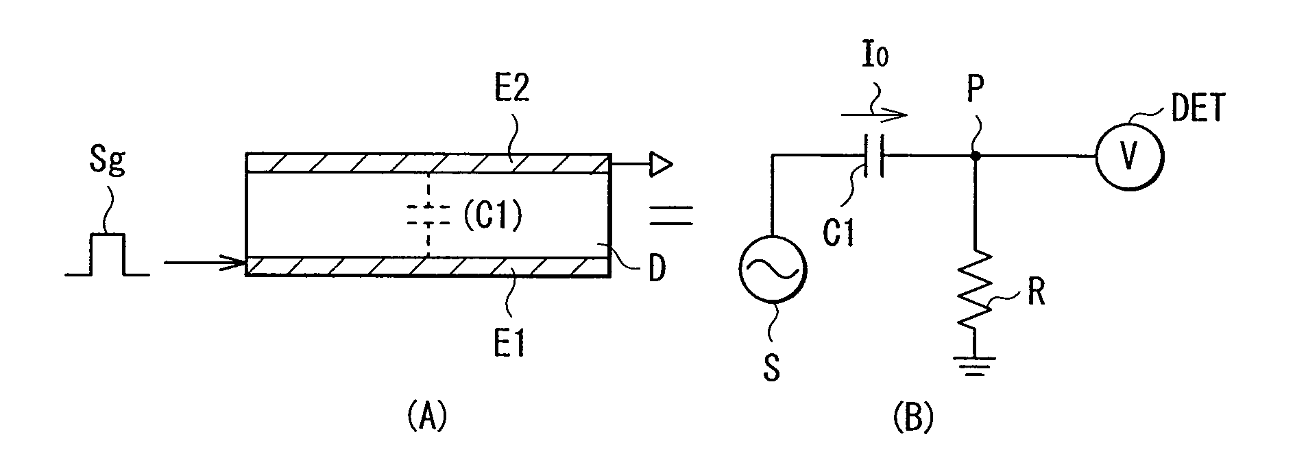
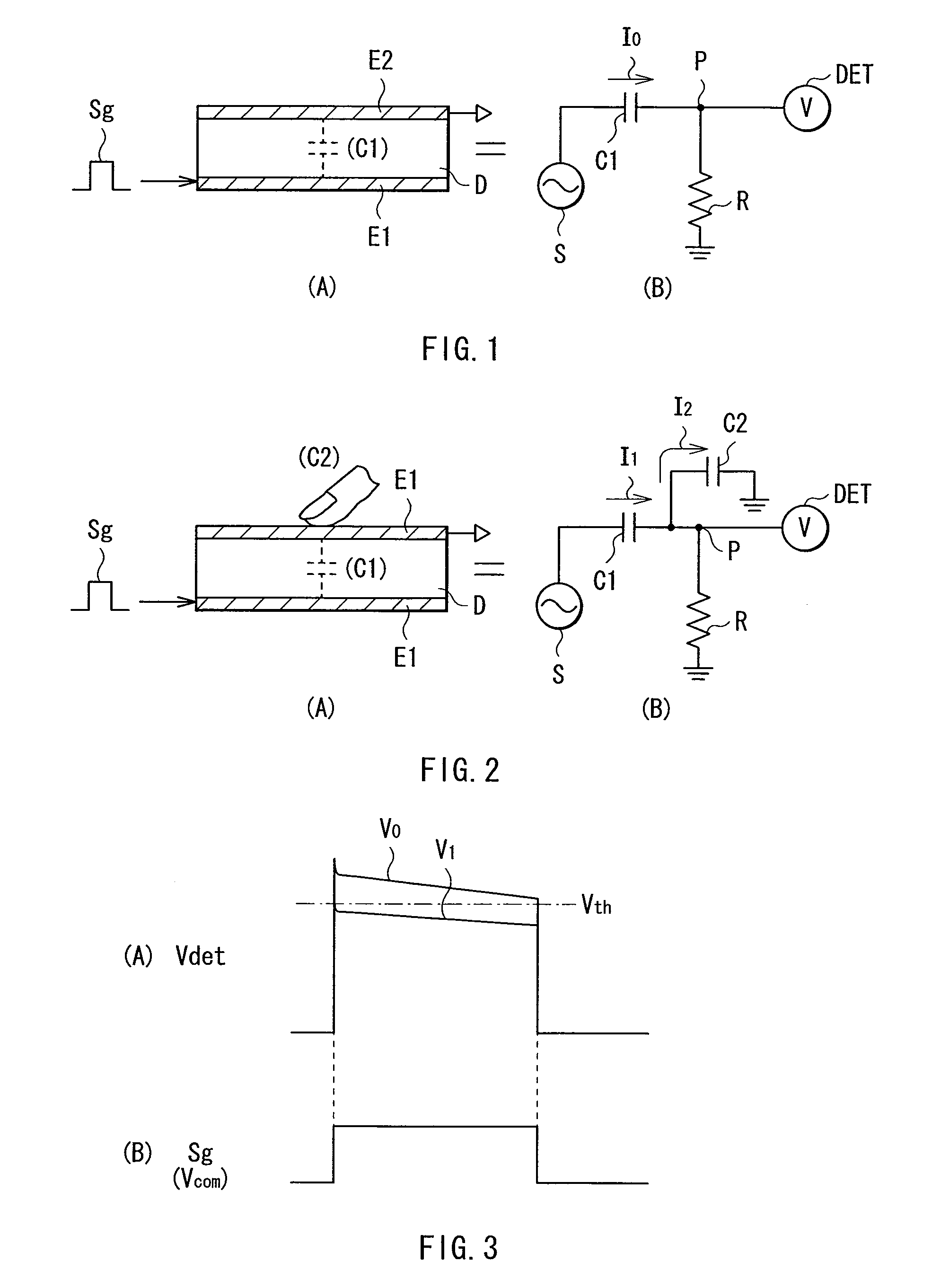
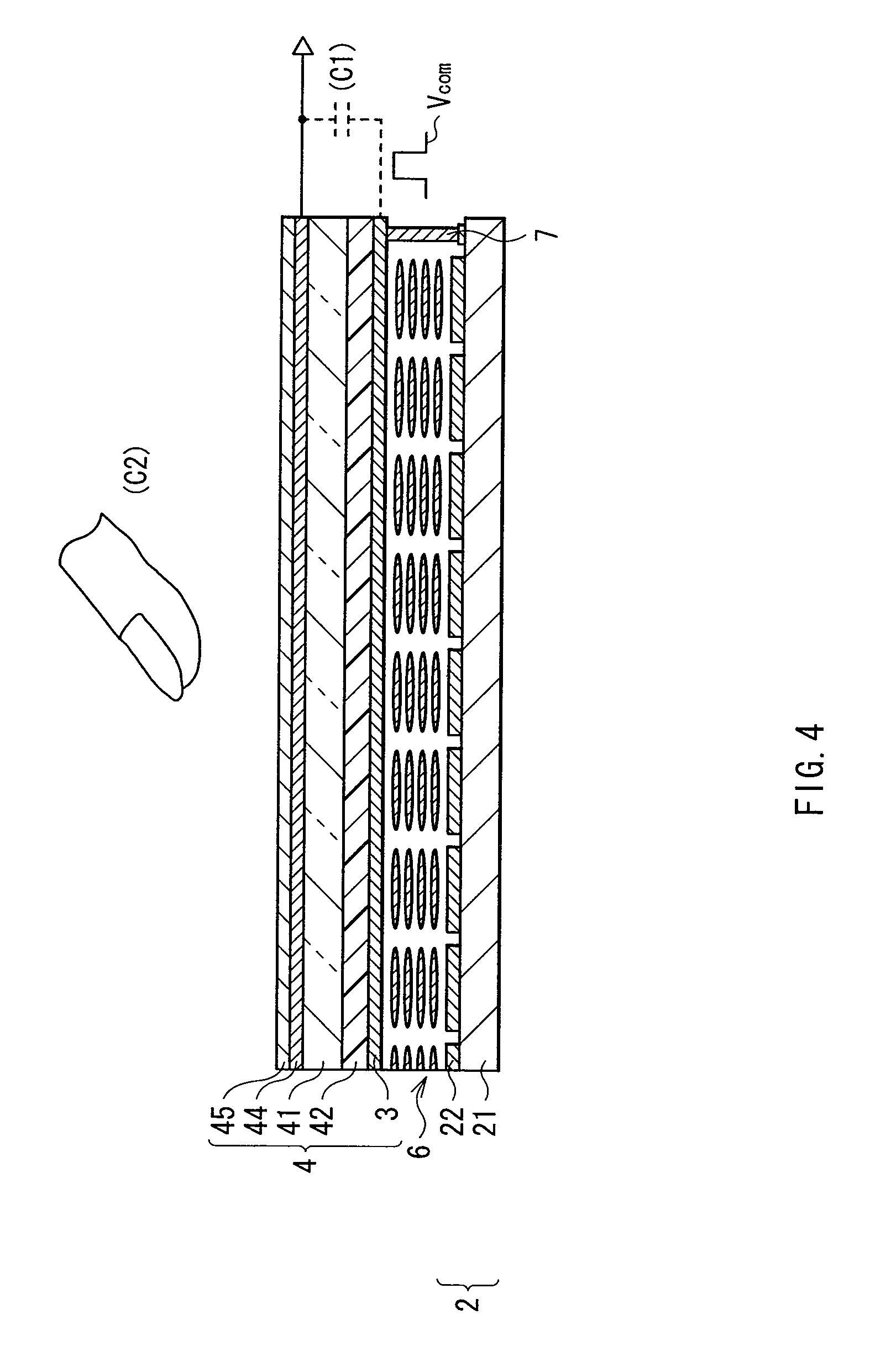
[0037]FIG. 4 illustrates the cross-sectional configuration of a main part of the display device with the touch sensor of the present embodiment. In this display device with the touch sensor, a liquid crystal display element is used as a display element, and a part of an electrode (common electrode 43, which will be described later) which is originally provided in this liquid crystal display element, and a drive signal for display (common drive signal Vcom, which will be described later) are used also for another purpose, thereby the capacitance type touch sensor is configured.

[0038]As illustrated in FIG. 4, the display device with the touch sensor includes a pixel substrate 2, an opposed substrate 4 facing this pixel substrate 2, and a liquid crystal layer 6 inserted between the pixel substrate 2 and the opposed substrate 4.

[0039]The pixel substrate 2 includes a TFT substrate 21 as a circuit substrate, and a plurality of pixel electrodes 22 disposed in a matrix form on this TFT subs...

second embodiment

[0058]Next, a second embodiment will be described. The present embodiment differs from the above-described first embodiment in that a liquid crystal element of a lateral electric field mode is used as a display element.

[0059]FIG. 9 illustrates the cross-sectional configuration of the main part of the display device with the touch sensor according to the present embodiment, and FIG. 10 illustrates its perspective configuration. In these views, same reference numerals as in FIG. 4 are used to indicate identical components, and thereby the description is appropriately omitted.

[0060]The display device with the touch sensor according to the present embodiment includes a pixel substrate 2A, an opposed substrate 4A facing this pixel substrate 2A, and the liquid crystal layer 6 inserted between the pixel substrate 2A and the opposed substrate 4A.

[0061]The pixel substrate 2A includes the TFT substrate 21, the common electrode 43 disposed on this TFT substrate 21, and the plurality of pixel e...

third embodiment

[0080]In the first embodiment and the second embodiment described above, the detection-electrode-for-the-sensor 44 is disposed in the display region. However, in the present embodiment, as illustrated in FIGS. 16 and 17, the detection-electrode-for-the-sensor 44 is provided in a region (frame region F) surrounding a display region D. FIG. 17 illustrates the plan configuration of the display device with the touch sensor of the present embodiment, and FIG. 16 illustrates the configuration as viewed from the direction of A-A arrow in FIG. 17.

[0081]In this display device with the touch sensor, both the common electrode 43 and the detection-electrode-for-the-sensor 44 are formed on a pixel substrate 2B side, and none of the common electrode 43 and the detection-electrode-for-the-sensor 44 are formed on the opposed substrate 4 side. Specifically, the common electrode 43 is formed on the TFT substrate 21, in the whole display region D. On the other hand, the detection-electrode-for-the-sen...


PUM


Abstract

A common electrode 43 for display, which is originally provided in a liquid crystal display element, is also used as one (drive electrode) of a pair of electrodes for a touch sensor, and the other (detection-electrode-for-the-sensor 44) of the pair of electrodes is newly formed. An existing common drive signal Vcom as a drive signal for display is used in common for a drive signal for the touch sensor. A capacitance is formed between the common electrode 43 and the detection-electrode-for-the-sensor 44, and touch detection is performed by utilizing a change of this capacitance caused by a finger touch of a user. Thus, a display device with a touch sensor is also applicable to a mobile device in which electric potential of the user is inconstant in many cases. The newly-provided electrode is only the detection-electrode-for-the-sensor 44, and it is unnecessary to newly prepare a drive signal for the touch sensor. Therefore, the configuration is simple.

Description

TECHNICAL FIELD[0001]The present invention relates to a display device such as a liquid crystal display device, and particularly relates to a display device with a touch sensor, which includes a touch sensor of capacitance type capable of inputting information by being touched with a user's finger or the like.BACKGROUND ART[0002]In recent years, a display device capable of inputting information by being provided with a contact detection device (hereinafter, referred to as a touch sensor), a so-called touch panel, directly mounted on a liquid crystal display device, and displaying various buttons on the liquid crystal display device, in substitution for typical buttons, has attracted attention. In the tendency that screens of mobile devices increase in size, this technique enables common arrangement of a display and buttons, and this brings a great merit such as space saving and reduction in the number of parts. However, in this technique, there is an issue that the thickness of a wh...

Claims


Application Information

Patent Timeline
Patent Type & Authority Applications(United States)
IPC IPC(8): G06F3/041
CPCG02F1/13338G02F1/134363G02F2001/134372G09G3/3648G06F3/0412G06F3/044G02F2201/12G06F3/0445G06F3/0443G06F3/0446G02F1/134372G06F2203/04107
Inventor NOGUCHI, KOJITAKAMA, DAISUKEKIDA, YOSHITOSHI
Owner JAPAN DISPLAY INC
Why Eureka
Try Eureka