Thin-film transistor array substrate, method of manufacturing the same, and liquid crystal display device

Active Publication Date: 2010-07-29
TRIVALE TECH LLC
View PDF17 Cites 24 Cited by
  • Summary
  • Abstract
  • Description
  • Claims
  • Application Information

AI Technical Summary

Benefits of technology

[0012]According to the exemplary aspects of the present invention described above, it is possible to provide a thin-film transistor array substrate, a method of manufacturing the same, and a liquid crystal display device which enable reduction of the number of photolithography processes without use of a half-tone mask.

Problems solved by technology

This raises a concern that manufacturing costs are high compared to a twisted nematic (TN) mode in which a TFT array substrate can be manufactured generally by five photolithography processes.
However, process control of a photolithography process with use of the half-tone mask is more complicated than that of a normal photolithography process, and there is a problem with stable mass production.
Further, the half-tone mask is more expensive than a normal mask, and there is also a problem with cost.

Method used


Image

  • Thin-film transistor array substrate, method of manufacturing the same, and liquid crystal display device
  • Thin-film transistor array substrate, method of manufacturing the same, and liquid crystal display device
  • Thin-film transistor array substrate, method of manufacturing the same, and liquid crystal display device

Examples


first exemplary embodiment

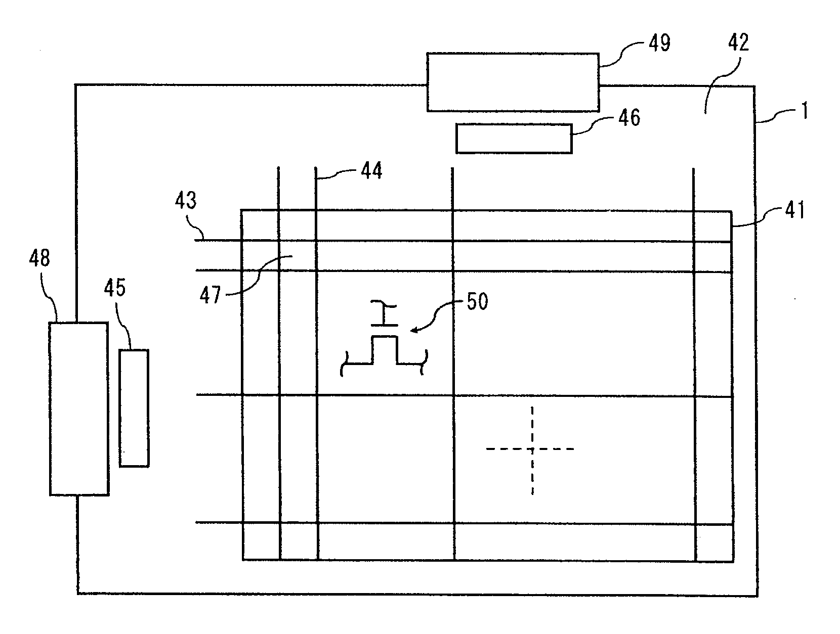
[0041]A liquid crystal display device according to a first exemplary embodiment of the present invention is described firstly with reference to FIG. 1. FIG. 1 is a front view showing a structure of a TFT array substrate that is used in the liquid crystal display device according to the first exemplary embodiment. The liquid crystal display device according to the first exemplary embodiment is an FFS mode liquid crystal display device in which a pixel electrode and a counter electrode are placed in the TFT array substrate. An overall structure of the liquid crystal display device is common among first to third exemplary embodiments described hereinbelow.

[0042]The liquid crystal display device according to the first exemplary embodiment includes a substrate 1. The substrate 1 is an array substrate such as a TFT array substrate, for example. The substrate 1 includes a display area 41 and a frame area 42 surrounding the display area 41. In the display area 41, a plurality of gate lines ...

second exemplary embodiment

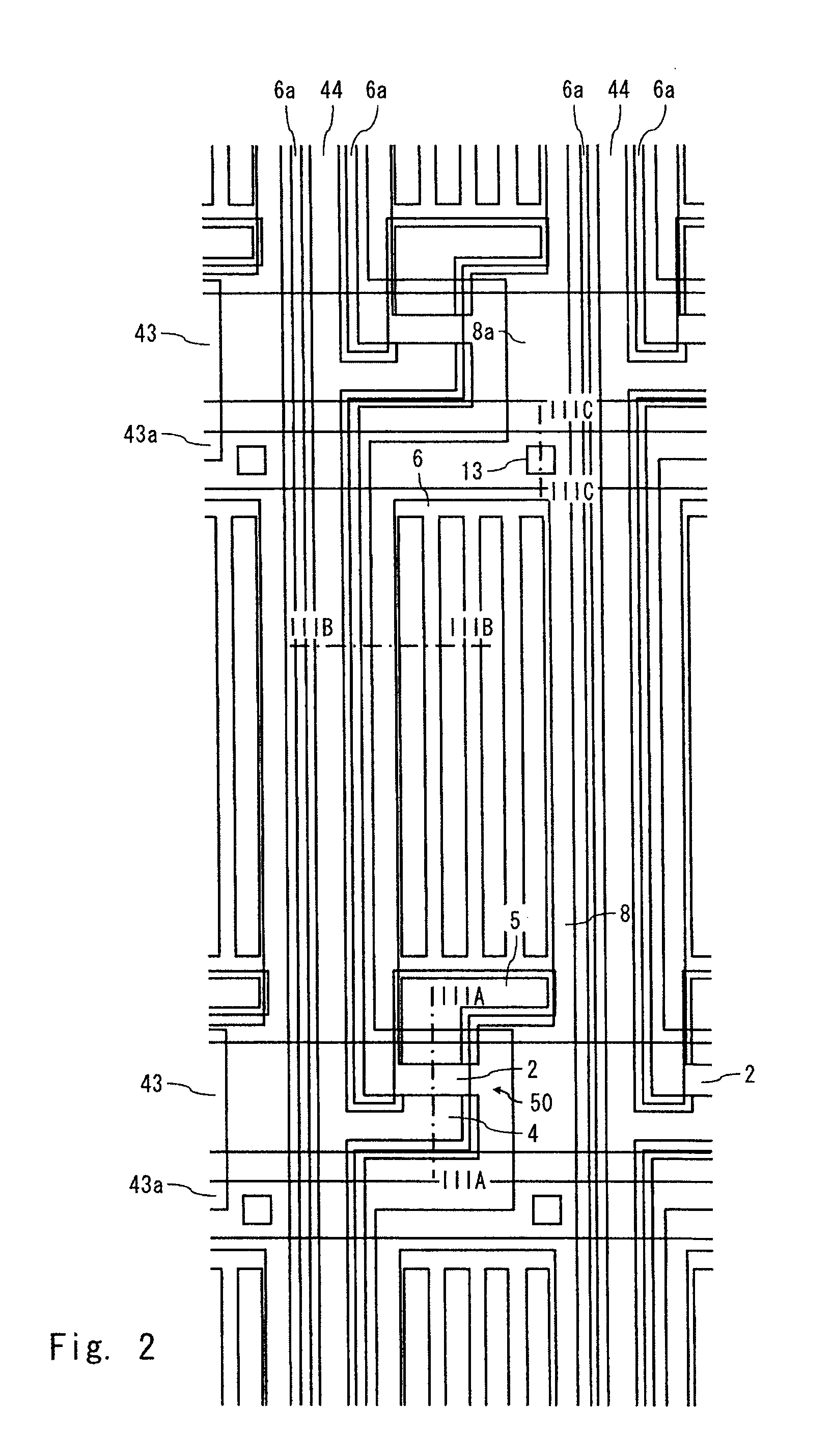
[0082]A pixel structure of a liquid crystal display device according to a second exemplary embodiment is described hereinafter with reference to FIG. 14 and FIGS. 15A to 15C. FIG. 14 is a plan view showing the pixel structure of the TFT array substrate according to the second exemplary embodiment. FIGS. 15A to 15C are cross-sectional views showing the pixel structure of the TFT array substrate according to the second exemplary embodiment. FIG. 14 shows one of the pixels 47 of the TFT array substrate. FIG. 15A is a cross-sectional view along line XVA-XVA in FIG. 14, FIG. 15B is a cross-sectional view along line XVB-XVB in FIG. 14, and FIG. 15C is a cross-sectional view along line XVC-XVC in FIG. 14. In the second exemplary embodiment, the shape of the counter electrode 8 is different from that of the first exemplary embodiment. The other structure is the same as that of the first exemplary embodiment and thus not redundantly described below.

[0083]In the second exemplary embodiment, t...

third exemplary embodiment

[0087]A pixel structure of a liquid crystal display device according to a third exemplary embodiment is described hereinafter with reference to FIG. 16 and FIGS. 17A and 17B. FIG. 16 is a plan view showing the pixel structure of the TFT array substrate according to the third exemplary embodiment. FIGS. 17A and 17B are cross-sectional views showing the pixel structure of the TFT array substrate according to the third exemplary embodiment. FIG. 16 shows one of the pixels 47 of the TFT array substrate. FIG. 17A is a cross-sectional view along line XVIIA-XVIIA in FIG. 16, and FIG. 17B is a cross-sectional view along line XVIIB-XVIIB in FIG. 16.

[0088]In the first exemplary embodiment, a signal is supplied to the counter electrode 8 of each pixel 47 from the common line 43a that is electrically connected to the counter electrode 8 through the contact hole 13 of each pixel 47. On the other hand, in the third exemplary embodiment, a signal is supplied to the counter electrode 8 from the per...


PUM


Abstract

A thin-film transistor array substrate includes a source line that is formed above a gate insulating layer covering a gate line, a semiconductor layer that is formed on the gate insulating layer and placed in a substantially whole area below a drain electrode, in a substantially whole area below a source electrode, in a substantially whole area below the source line and in a position opposite to the gate electrode, a pixel electrode that is formed directly on the drain electrode, a transparent conductive pattern that is formed directly on the source electrode and the source line in the same layer as the pixel electrode, and a counter electrode that is formed on an interlayer insulating layer covering the pixel electrode and the transparent conductive pattern and generates a fringe electric field with the pixel electrode.

Description

INCORPORATION BY REFERENCE[0001]This application is based upon and claims the benefit of priorities from Japanese patent applications Nos. 2009-012852 filed on Jan. 23, 2009 and 2009-281645 filed on Dec. 11, 2009, the disclosure of which is incorporated herein in its entirety by reference.BACKGROUND OF THE INVENTION[0002]1. Field of the Invention[0003]The present invention relates to a thin-film transistor array substrate, a method of manufacturing the same, and a liquid crystal display device. Particularly, the present invention relates to a thin-film transistor array substrate to be used for a fringe-field switching mode liquid crystal display device, a method of manufacturing the same, and a liquid crystal display device.[0004]2. Description of Related Art[0005]A fringe-field switching (FFS) mode of a liquid crystal display device is a display technique that displays an image by applying a fringe electric field to liquid crystals filled between substrates placed opposite to each ...

Claims


Application Information

Patent Timeline
IPC IPC(8): H01L33/00H01L31/00
CPCG02F1/136286G02F2001/134372H01L27/1288H01L27/124H01L29/458G02F1/134372
Inventor NAGANO, SHINGOMASUTANI, YUICHI
Owner TRIVALE TECH LLC
Why Eureka
Try Eureka